CHA5295
Ref. : DSCHA52953125 - 05 May 03
1/8
Specifications subject to change without notice
United Monolithic Semiconductors S.A.S.
Route DÈpartementale 128 - B.P.46 - 91401 Orsay Cedex France
Tel. : +33 (0)1 69 33 03 08 - Fax : +33 (0)1 69 33 03 09
24.5-26.5GHz High Power Amplifier
GaAs Monolithic Microwave IC
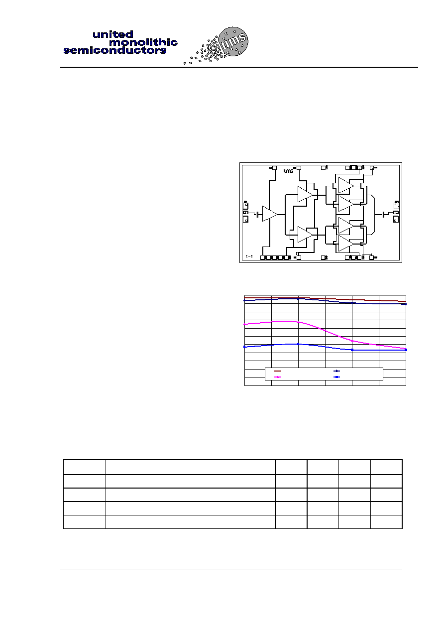
Description
The CHA5295 is a high gain three-stage
monolithic high power amplifier. It is designed for
a wide range of applications, from military to
commercial communication systems.
The
backside of the chip is both RF and DC grounds.
This help simplifies the assembly process.
The circuit is manufactured with a PM-HEMT
process, 0.25µm gate length, via holes through
the substrate, air bridges and electron beam gate
lithography.
It is available in chip form.
Main Features
Performances : 24.5-26.5GHz
31dBm output power @ 1dB comp.
18 dB
±
1dB gain
DC power consumption, 800mA @ 6V
Chip size : 4.01 x 2.52 x 0.05 mm
Vd1 Vd2 Vg3 Vd3
Vg1 Vg2 Vd2 Vg3 Vd3
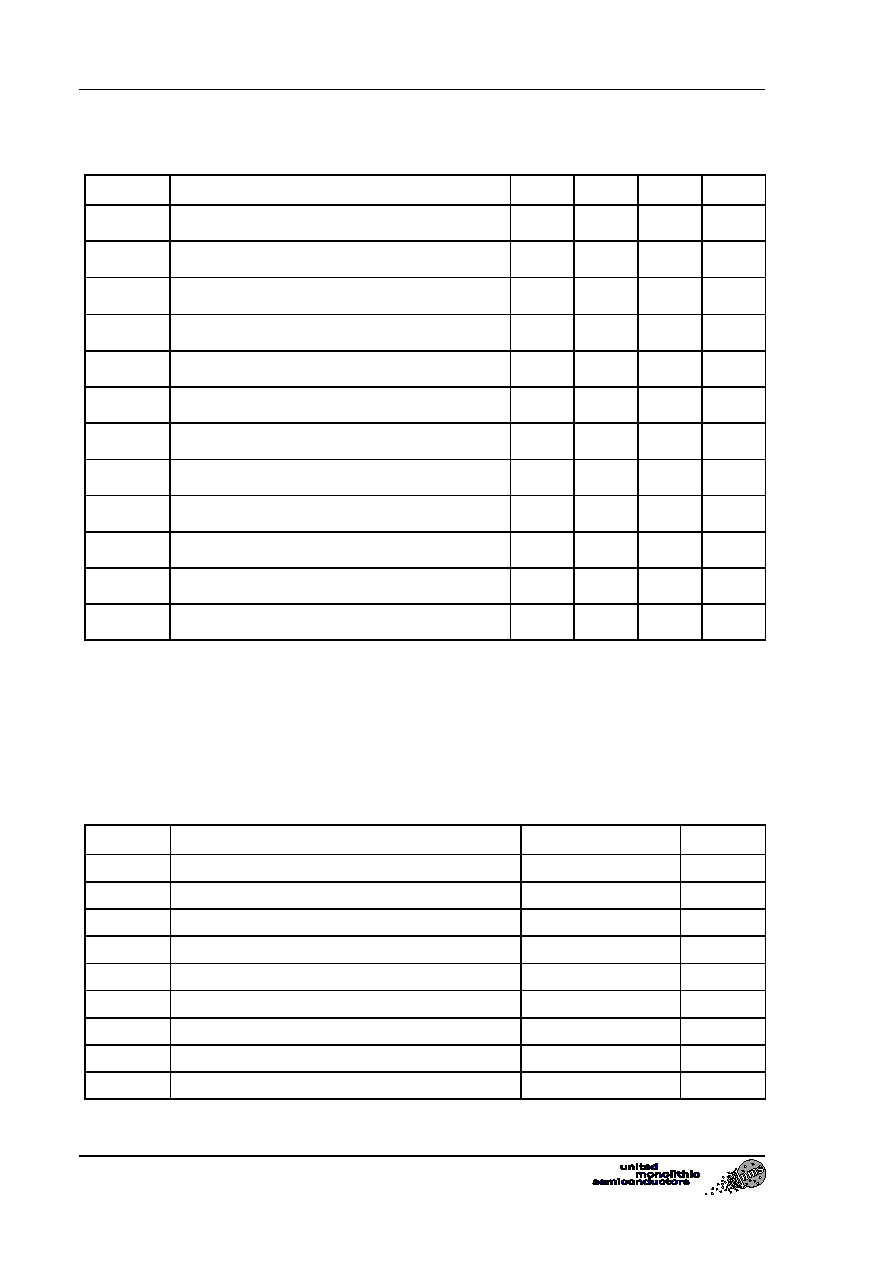
10
12
14
16
18
20
22
24
26
28
30
32
24,5
25
25,5
26
26,5
27
27,5
Frequency (GHz)
Pout@3dB (dBm)
Pout@1dB (dBm)
PAE@1dB (%)
Linear Gain (dB)
Typical on jig Measurements
Main Characteristics
Tamb. = 25∞C
Symbol Parameter Min
Typ
Max
Unit
Fop
Operating frequency range
24.5
26.5
GHz
G
Small signal gain
17
18
dB
P1dB
Output power at 1dB gain compression
30
31
dBm
Id Bias
current
800
mA
ESD Protection : Electrostatic discharge sensitive device. Observe handling precautions !
CHA5295
24.5-26.5GHz High Power Amplifier
Ref. : DSCHA52953125 - 05 May 03
2/8
Specifications subject to change without notice
Route DÈpartementale 128 , B.P.46 - 91401 ORSAY Cedex - FRANCE
Tel.: +33 (0)1 69 33 03 08 - Fax : +33 (0)1 69 33 03 09
Electrical Characteristics
Tamb = +25∞C, Vd = 6V Id #800mA
Symbol Parameter Min
Typ
Max
Unit
Fop
Operating frequency range (1)
24.5
26.5
GHz
G
Small signal gain (1)
17
18
dB
G
Small signal gain flatness (1)
±
1
dB
Is
Reverse isolation
50
dB
P1dB
Pulsed output power at 1dB compression (1)
30
31
dBm
P03
Output power at 3dB gain compression (1)
31.5
dBm
IP3 3
rd
order intercept point (2) (3)
41
dBm
PAE
Power added efficiency at 1dB comp.
20
%
VSWRin Input VSWR
3.5:1
VSWRout Output
VSWR
2:1
Tj
Junction temperature for 80∞C backside
+155
∞C
Id
Bias current @ small signal
800
1000
mA
(1) These values are representative for pulsed on-wafer measurements that are made without
bonding wires at the RF ports.
(2) Value representative for CW on jig measurement.
(3) Linearity could be improved with a biasing point around 600mA ( see curves on next pages)
Absolute Maximum Ratings
Tamb. = 25∞C (1)
Symbol Parameter
Values
Unit
Vd
Maximum drain bias voltage with Pin max=12dBm
+6.25
V
Id
Maximum drain bias current
1400
mA
Vg
Gate bias voltage
-2.5 to +0.4
V
Ig
Gate bias current
-5 to +5
mA
Vdg
Maximum drain to gate voltage (Vd - Vg)
+8.0
V
Pin
Maximum input power overdrive (2)
+15
dBm
Tch
Maximum channel temperature
+175
∞C
Ta
Operating temperature range
-40 to +80
∞C
Tstg
Storage temperature range
-55 to +125
∞C
(1) Operation of this device above anyone of these parameters may cause permanent damage.
(2) Duration < 1s.
24.5-26.5GHz High Power Amplifier
CHA5295
Ref. : DSCHA52953125 - 05 May 03
3/8
Specifications subject to change without notice
Route DÈpartementale 128 , B.P.46 - 91401 ORSAY Cedex - FRANCE
Tel.: +33 (0)1 69 33 03 08 - Fax : +33 (0)1 69 33 03 09
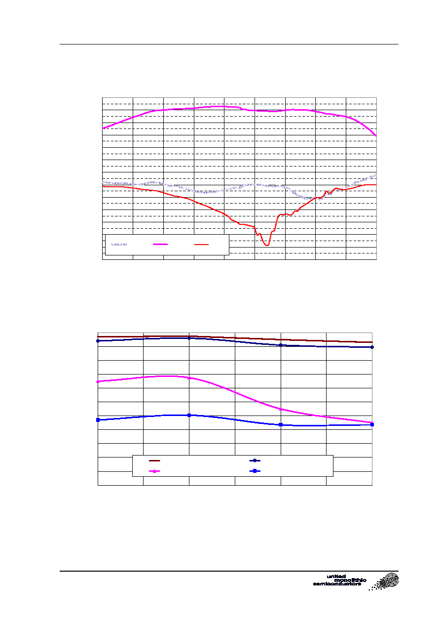
Typical on Jig Measurements
Bias conditions: Vd=6V, Vg tuned for Id #800mA
-30
-26
-22
-18
-14
-10
-6
-2
2
6
10
14
18
22
22
23
24
25
26
27
28
29
30
31
Frequency (GHz)
(d
B)
S11
S21
S22
Linear Gain & Return Losses versus frequency
10
12
14
16
18
20
22
24
26
28
30
32
24,5
25
25,5
26
26,5
27
27,5
Frequency (GHz)
Pout@3dB (dBm)
Pout@1dB (dBm)
PAE@1dB (%)
Linear Gain (dB)
Linear Gain, Output power @ 1dB & 3dB compression,
PAE @ 1dB compression
CHA5295
24.5-26.5GHz High Power Amplifier
Ref. : DSCHA52953125 - 05 May 03
4/8
Specifications subject to change without notice
Route DÈpartementale 128 , B.P.46 - 91401 ORSAY Cedex - FRANCE
Tel.: +33 (0)1 69 33 03 08 - Fax : +33 (0)1 69 33 03 09
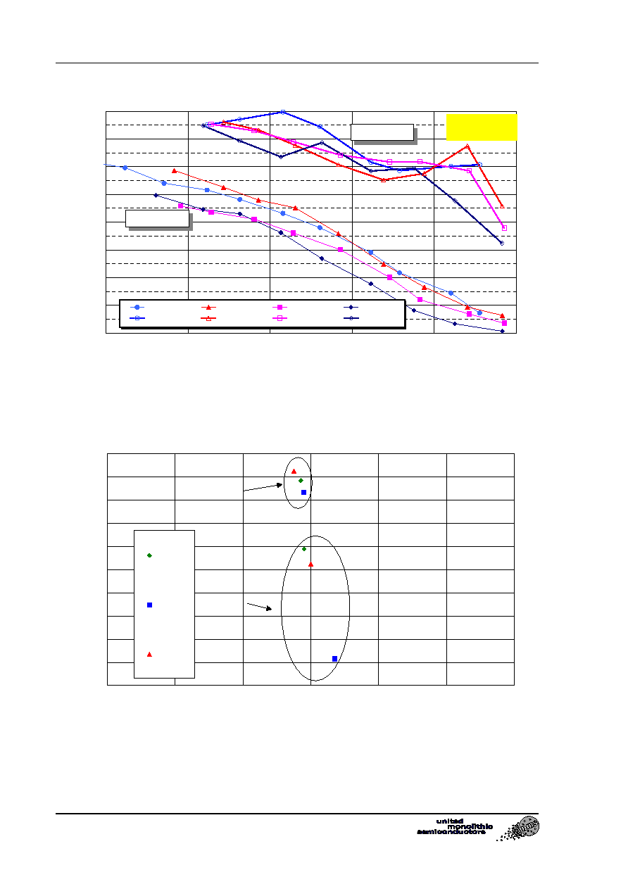
26
30
34
38
42
46
50
54
58
16
18
20
22
24
26
Pout (dBm)
24GHz
25GHz
26GHz
27GHz
6V, 600mA
C/I3 (dBc)
C/I5 (dBc)
C/I3 & C/I5 versus DCL* Output Power
30
32
34
36
38
40
42
44
46
48
50
12
14
16
18
20
22
24
Pout (dBm)
C/I
3
(
dBc
)
+25∞C
-35∞C
+75∞C
600mA
800mA
C/I3 versus drain current & temperature @ 25.5GHz
DCL: Double Carrier Level

24.5-26.5GHz High Power Amplifier
CHA5295
Ref. : DSCHA52953125 - 05 May 03
5/8
Specifications subject to change without notice
Route DÈpartementale 128 , B.P.46 - 91401 ORSAY Cedex - FRANCE
Tel.: +33 (0)1 69 33 03 08 - Fax : +33 (0)1 69 33 03 09
10
12
14
16
18
20
22
24
26
28
30
20
21
22
23
24
25
26
27
28
29
30
31
32
33
34
Output power (dBm)
Gai
n
(
d
B)
+25∞C - 600mA
-40∞C - 600mA
+85∞C - 600mA
+25∞C - 800mA
-40∞C - 800mA
+85∞C - 800mA
Output power versus temperature & Drain current @ 25.5GHz