 | –≠–ª–µ–∫—Ç—Ä–æ–Ω–Ω—ã–π –∫–æ–º–ø–æ–Ω–µ–Ω—Ç: CHA5297 | –°–∫–∞—á–∞—Ç—å:  PDF PDF  ZIP ZIP |

CHA5297
Ref. : DSCHA52972149 - 29-May-02
1/4
Specifications subject to change without notice
United Monolithic Semiconductors S.A.S.
Route DÈpartementale 128 - B.P.46 - 91401 Orsay Cedex France
Tel. : +33 (0)1 69 33 03 08 - Fax : +33 (0)1 69 33 03 09
37-40GHz High Power Amplifier
GaAs Monolithic Microwave IC
Description
The CHA5297 is a three-stage monolithic high
power amplifier. It is designed for a wide range
of applications, from military to commercial
communication systems. The backside of the
chip is both RF and DC grounds. This helps
simplify the assembly process.
The circuit is manufactured with a PM-HEMT
process, 0.15µm gate length, via holes through
the substrate, air bridges and electron beam
gate lithography.
It is available in chip form.
Main Features
Performances : 37-40GHz
28dBm output power @ 1dB comp. gain
10 dB
±
1dB gain
DC power consumption, 1.6A @ 3.5V
Chip size : 4.16 x 2.6 x 0.05 mm
Vd1 Vd2 Vg3 Vd3
Vg1 Vg2 Vd2 Vg3 Vd3
IN
OUT
Main Characteristics
Tamb. = 25∞C
Symbol Parameter Min
Typ
Max
Unit
Fop
Operating frequency range
37
40
GHz
G
Small signal gain
10
dB
P1dB
Output power at 1dB gain compression
28
dBm
Id
Bias
current
1.6 A
ESD Protection : Electrostatic discharge sensitive device. Observe handling precautions !

CHA5297
37-40GHz High Power Amplifier
Ref. : DSCHA52972149 - 29-May-02
2/4
Specifications subject to change without notice
Route DÈpartementale 128 , B.P.46 - 91401 ORSAY Cedex - FRANCE
Tel.: +33 (0)1 69 33 03 08 - Fax : +33 (0)1 69 33 03 09
Electrical Characteristics
Tamb = +25∞C, Vd = 3.5V Id =1.6A
Symbol Parameter Min
Typ
Max
Unit
Fop
Operating frequency range (1)
37
40
GHz
G
Small signal gain (1)
10
dB
G
Small signal gain flatness (1)
±
1
dB
Is
Reverse isolation
40
dB
P1dB
Pulsed output power at 1dB compression (1)
28
dBm
P03
Output power at 3dB gain compression (1)
29
dBm
VSWRin Input VSWR (2)
3:1
VSWRout Output VSWR (2)
3.5:1
Tj
Junction temperature for 80∞C backside
152
∞C
Id
Bias current @ small signal
1.6
2
A
(1) These values are representative for pulsed on-wafer measurements that are made without
bonding wires at the RF ports.
(2) Value representative for CW on jig measurement.
Absolute Maximum Ratings
Tamb. = 25∞C (1)
Symbol Parameter
Values
Unit
Vd
Maximum drain bias voltage with Pin max=18dBm
+4.0
V
Id
Maximum drain bias current
2.2
A
Vg
Gate bias voltage
-2 to +0.4
V
Ig
Gate bias current
-5.5 to +5.5
mA
Vdg
Maximum drain to gate voltage (Vd - Vg)
+6.0
V
Pin
Maximum input power overdrive (2)
+22
dBm
Tch
Maximum channel temperature
+175
∞C
Ta
Operating temperature range
-40 to +80
∞C
Tstg
Storage temperature range
-55 to +125
∞C
(1) Operation of this device above anyone of these parameters may cause permanent damage.
(2) Duration < 1s.
37-40GHz High Power Amplifier
CHA5297
Ref. : DSCHA52972149 - 29-May-02
3/4
Specifications subject to change without notice
Route DÈpartementale 128 , B.P.46 - 91401 ORSAY Cedex - FRANCE
Tel.: +33 (0)1 69 33 03 08 - Fax : +33 (0)1 69 33 03 09
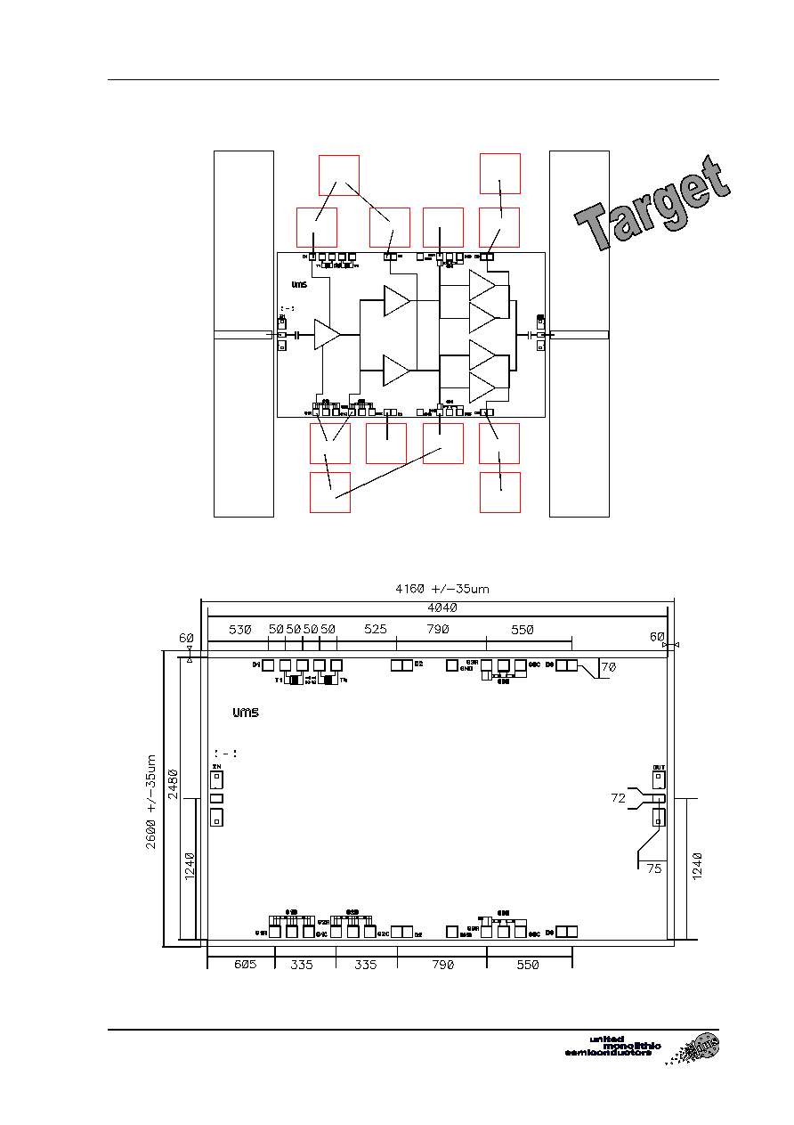
Chip Assembly and Mechanical Data
120pF
120pF
120pF
120pF
120pF
120pF
120pF
120pF
10nF
10nF
10nF
10nF
To Vd1,2 DC Drain supply feed To Vd3 DC Drain supply feed
To Vg1,2,3 DC Gate supply feed
To Vd3 DC Drain supply feed
RF IN
RF OUT
Note : Supply feed should be capacitively bypassed. 25µm diameter gold wire is to be prefered.
Bonding pad positions.
( Chip thickness : 50µm. All dimensions are in micrometers )
CHA5297
37-40GHz High Power Amplifier
Ref. : DSCHA52972149 - 29-May-02
4/4
Specifications subject to change without notice
Route DÈpartementale 128 , B.P.46 - 91401 ORSAY Cedex - FRANCE
Tel.: +33 (0)1 69 33 03 08 - Fax : +33 (0)1 69 33 03 09
Application note
Bias operation sequence:
ON: Supply Gate voltage
Supply Drain voltage
OFF: Cut off Drain voltage
Cut off Gate voltage
Due to 50µm thickness, specific care is requested for the handling and assembly.
Ordering Information
Chip form
:
CHA5297-99F/00
Information furnished is believed to be accurate and reliable. However United Monolithic Semiconductors
S.A.S. assumes no responsability for the consequences of use of such information nor for any infringement of
patents or other rights of third parties which may result from its use. No license is granted by implication or
otherwise under any patent or patent rights of United Monolithic Semiconductors S.A.S.. Specifications
mentioned in this publication are subject to change without notice. This publication supersedes and replaces all
information previously supplied. United Monolithic Semiconductors S.A.S. products are not authorised for use
as critical components in life support devices or systems without express written approval from United
Monolithic Semiconductors S.A.S.