 | –≠–Ľ–Ķ–ļ—ā—Ä–ĺ–Ĺ–Ĺ—č–Ļ –ļ–ĺ–ľ–Ņ–ĺ–Ĺ–Ķ–Ĺ—ā: CHA7010 | –°–ļ–į—á–į—ā—Ć:  PDF PDF  ZIP ZIP |
Document Outline
- Main Features
- ESD Protections : Electrostatic discharge sensitive device observe handling precautions !
- Typical measured characteristics
- Typical measured characteristics
- Pin number
- 1
- NC
- Collector control current port
- 5, 7, 10, 12, 14, 19, 16, 21
- 6, 11, 15, 20
- 13
CHA7010
Ref. : DSCHA70102175 -24-June-02
1/7
Specifications subject to change without notice
United Monolithic Semiconductors S.A.S.
Route Dťpartementale 128 - B.P.46 - 91401 Orsay Cedex France
Tel. : +33 (0)1 69 33 03 08 - Fax : +33 (0)1 69 33 03 09
X-band GaInP HBT High Power Amplifier
GaAs Monolithic Microwave IC
Description
The CHA7010 is a monolithic two stage
GaAs high power amplifier designed for X
band applications.
This device is manufactured using a GaInP
HBT process, including, via holes through
the substrate and air bridges. A nitride
layer protects the transistors and the
passive components. Special heat removal
techniques are implemented to guarantee
high reliability.
To simplify the assembly process;
∑
the backside of the chip is both RF and
DC grounded
∑
bond pads and back side are gold
plated for compatibility with eutectic die
attach method and thermo-sonic or
thermo-compression bonding process.
Main Features
n
10W output power
n
High gain : > 18dB @ 10GHz
n
High PAE : > 35% @ 10GHz
n
On-chip bias control
n
Linear collector current control
n
High impedance interface for pulse
mode
n
Temperature compensated
n
Chip size: 4.74 x 4.36 x 0.1 mm
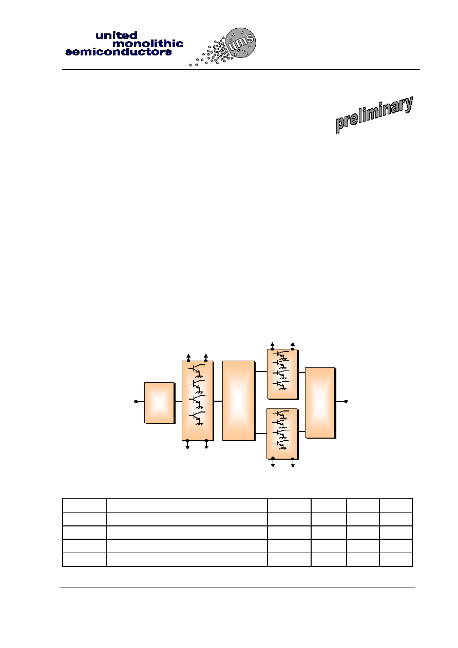
Vctr
Vc
Vctr
Vc
Vctr
Vc
Vctr
Vc
Inter-stage
Input
Matching
Network
Output
Combiner
Main Characteristics
Tamb = +25įC
Symbol Parameter Min
Typ
Max
Unit
F_op
Operating frequency range
8.4
9.4
10.4
GHz
P_sat
Saturated output power
10
W
P_1dBc
Output power @ 1dBc
8
W
G_lin Linear
gain
18
dB
ESD Protections : Electrostatic discharge sensitive device observe handling precautions !
X-band High Power Amplifier
CHA7010
Ref. : DSCHA70102175 -24-June-02
2/7
Specifications subject to change without notice
Route Dťpartementale 128 , B.P.46 - 91401 ORSAY Cedex - FRANCE
Tel.: +33 (0)1 69 33 03 08 - Fax : +33 (0)1 69 33 03 09
Electrical Characteristics
Tamb = 25įC, Vc=9V, Vctr=5.5V, Pulse width=80Ķs , Duty cycle = 30%
Symbol Parameter
Min
Typ
Max
Unit
F_op
Operating frequency
8.4
9.4
10.4
GHz
G_lin_1
Linear gain (8.4 to 9.4GHz)
14
16
dB
G_lin_2
Linear gain (9.4 to 10.4GHz)
16
18
dB
G_lin_T
Linear gain variation versus temperature
-0.035
dB/įC
RL_in
Input Return Loss
8
12
dB
RL_out
Output Return Loss
6
12
dB
P_sat_1
Saturated output power (8.4 to 9.8GHz)
39
40
dBm
P_sat_2
Saturated output power (9.8 to 10.4GHz)
38
39
dBm
P_sat_T
Saturated output power variation versus
temperature
-0.01 dB/įC
P_1dBc_1
Output power @ 1dBc (8.4 to 9.8GHz)
38
39
dBm
P_1dBc_2
Output power @ 1dBc (9.8 to 10.4GHz)
37
38
dBm
PAE_sat
Power Added Efficiency in saturation
30
35
%
PAE_1dBc
Power Added Efficiency @ 1dBc
27
32
%
Vc
Power supply voltage
9
V
Ic
Power supply quiescent current (1)
2.4
A
Vctr
Collector current control voltage
5.5
V
Zctr
Vctr input port impedance (2)
350
Ohm
Top
Operating temperature range (3)
-30
+80
įC
(1) This parameter is fixed by Vctr
(2) This value corresponds to the 4 ports in parallel (Pin 4, 9, 17, 22)
(3) The reference is the back-side of the chip
Absolute Maximum Ratings (1)
Tamb = 25įC
Symbol Parameter
Values
Unit
Cmp Compression
level
6 dB
Vc
Power supply voltage
10
V
Ic
Power supply quiescent current
2.8
A
Ic_sat
Power supply current in saturation
3.5
A
Vctr
Collector current control voltage
6.5
V
Tstg
Storage temperature range
-55 to +125
įC
(1)
Operation of this device above anyone of these parameters may cause permanent damage.
X-band High Power Amplifier
CHA7010
Ref. : DSCHA70102175 -24-June-02
3/7
Specifications subject to change without notice
Route Dťpartementale 128 , B.P.46 - 91401 ORSAY Cedex - FRANCE
Tel.: +33 (0)1 69 33 03 08 - Fax : +33 (0)1 69 33 03 09
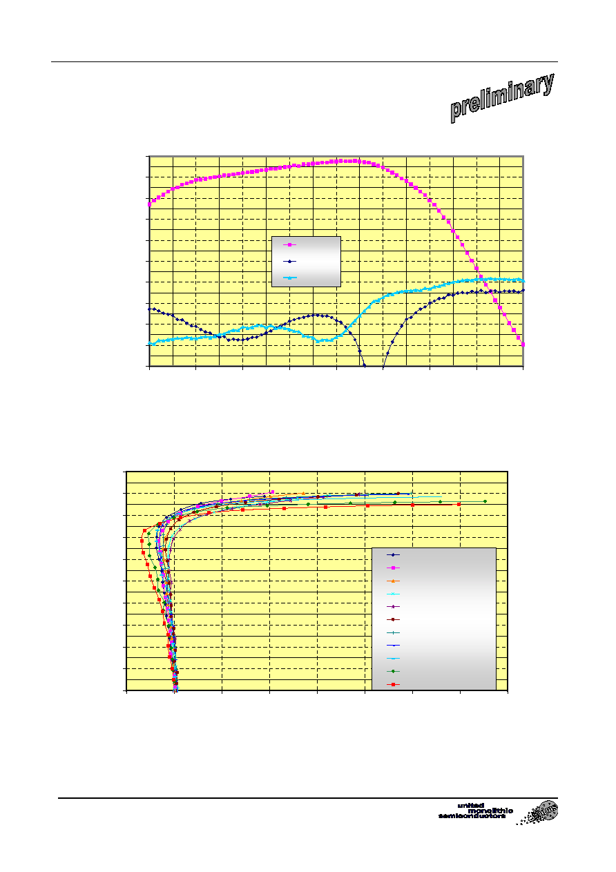
Typical measured characteristics
Measurements in test fixture :
Tamb=25įC, Vc=9V, Vctr=5.5V, Pulse width=80Ķs , Duty cycle = 30%
-20
-16
-12
-8
-4
0
4
8
12
16
20
8
8,5
9
9,5
10
10,5
11
11,5
12
Frequency(GHz)
S21,
S11,
S22 (dB)
db(S21)
db(S11)
db(S22)
S-parameters
22
24
26
28
30
32
34
36
38
40
42
-1
0
1
2
3
4
5
6
7
Compression level (dB)
Output power
(
d
Bm)
Pout @ 8,4 GHz
Pout @ 8,6 GHz
Pout @ 8,8 GHz
Pout @ 9 GHz
Pout @ 9.2 GHz
Pout @ 9.4 GHz
Pout @ 9.6 GHz
Pout @ 9.8 GHz
Pout @ 10 GHz
Pout @ 10.2 GHz
Pout @ 10.4 GHz
Output power versus compression level : F= 8.4 to 10.4GHz
X-band High Power Amplifier
CHA7010
Ref. : DSCHA70102175 -24-June-02
4/7
Specifications subject to change without notice
Route Dťpartementale 128 , B.P.46 - 91401 ORSAY Cedex - FRANCE
Tel.: +33 (0)1 69 33 03 08 - Fax : +33 (0)1 69 33 03 09
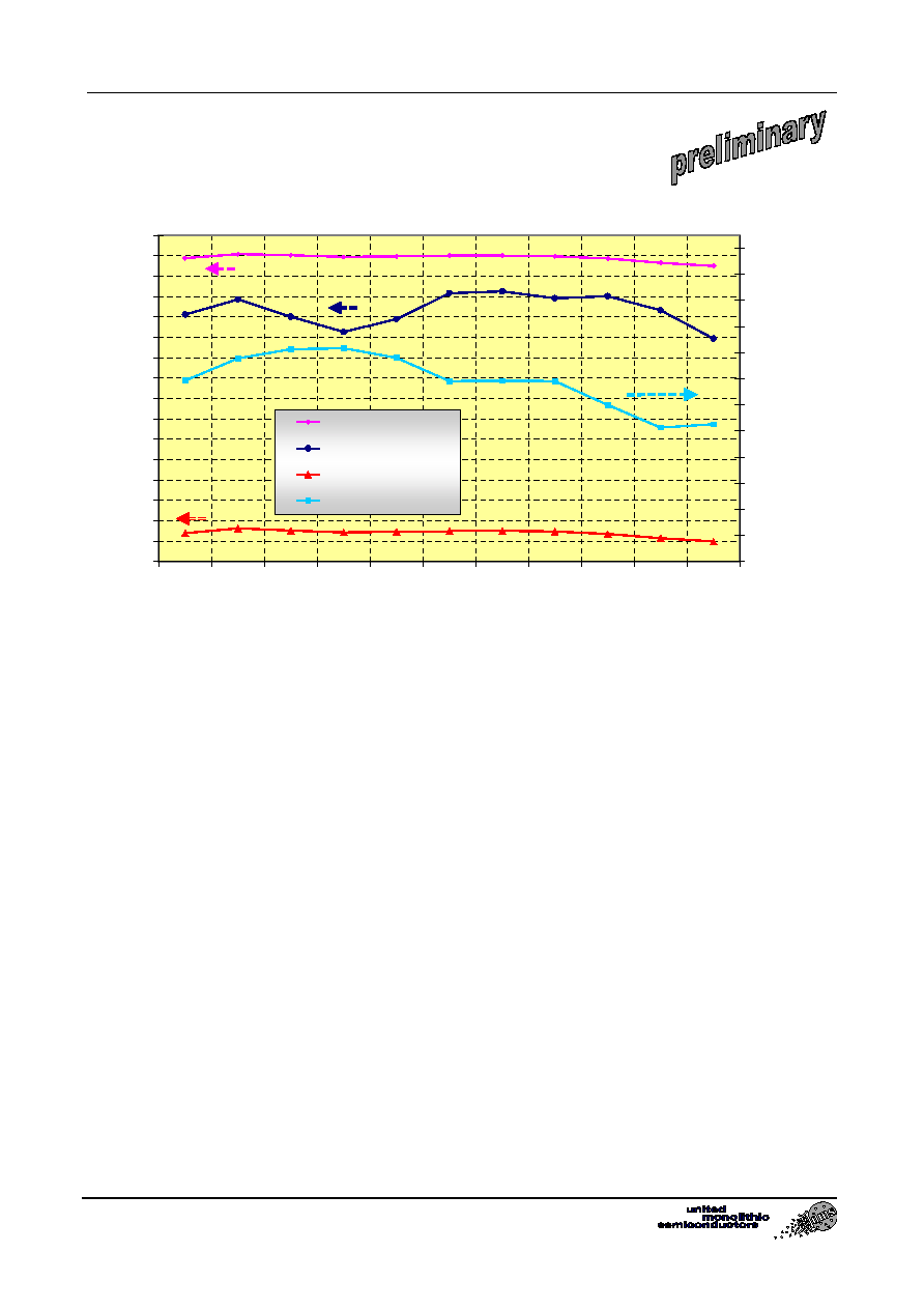
Typical measured characteristics
Measurements in test fixture :
Tamb=25įC, Vc=9V, Vctr=5.5V, Pulse width=80Ķs , Duty cycle = 30%
10
12
14
16
18
20
22
24
26
28
30
32
34
36
38
40
42
8,4
8,6
8,8
9
9,2
9,4
9,6
9,8
10
10,2
10,4
Frequency (GHz)
P
_
o
u
t(d
Bm)
,
P
ae(%),
Gai
n
(d
B)
1500
1700
1900
2100
2300
2500
2700
2900
3100
3300
3500
3700
3900
Col
l
ector current (mA)
Pout @ pin = 27 dBm
Pae @ pin = 27 dBm
gain @ pin = 27 dBm
Ic @ pin = 27 dBm
Saturated output power, PAE, Gain and collector current versus frequency
X-band High Power Amplifier
CHA7010
Ref. : DSCHA70102175 -24-June-02
5/7
Specifications subject to change without notice
Route Dťpartementale 128 , B.P.46 - 91401 ORSAY Cedex - FRANCE
Tel.: +33 (0)1 69 33 03 08 - Fax : +33 (0)1 69 33 03 09
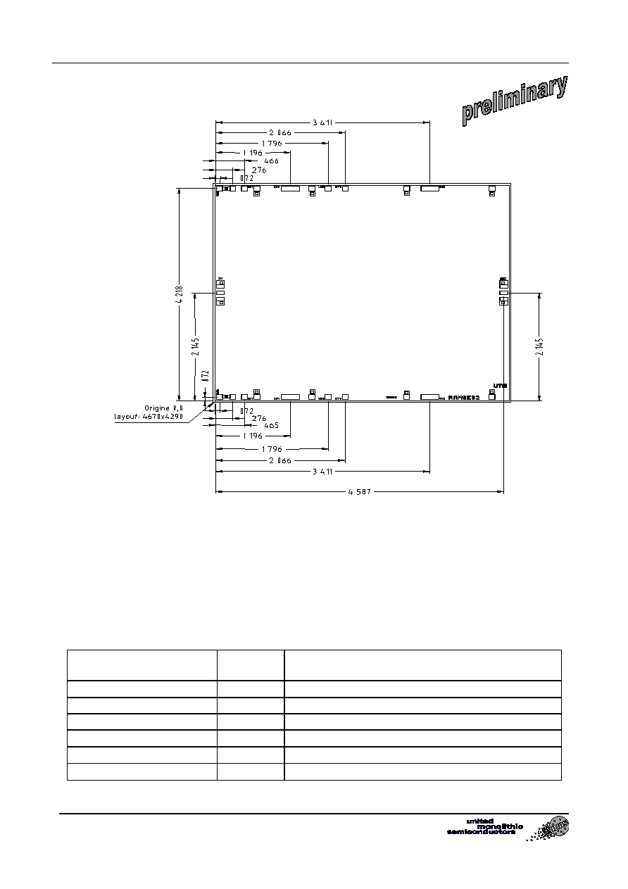
Dimensions and Pad allocation
1
2 3 4 5
6
7
8
9
10
11
12
13
24 23 22 21
20
19 18 17
16
15
14
Unit = Ķm
External chip size (including saw streets) = 4740 x 4360 +/- 35
Chip thickness = 100 +/- 10
HF pads (1, 13) = 118 x 68
DC pads (4, 9, 17, 22) = 96 x 96
DC pads (6, 11, 15, 20) = 288 x 96
Pin number
Pin name
Description
1
IN
Input RF port
2, 3, 8, 18, 23, 24
NC
4, 9, 17, 22
Vctr
Collector control current port
5, 7, 10, 12, 14, 19, 16, 21
GND
Ground (NC)
6, 11, 15, 20
Vc
Power supply voltage
13 OUT
Output RF port