 | –≠–ª–µ–∫—Ç—Ä–æ–Ω–Ω—ã–π –∫–æ–º–ø–æ–Ω–µ–Ω—Ç: CHM1291 | –°–∫–∞—á–∞—Ç—å:  PDF PDF  ZIP ZIP |

CHM1291
Ref. : DSCHM12912266 - 23-Sept.-02
1/6
Specifications subject to change without notice
Route DÈpartementale 128 , B.P.46 - 91401 ORSAY Cedex - FRANCE
Tel.: +33 (0)1 69 33 03 08 - Fax : +33 (0)1 69 33 03 09
25-32GHz Single Side Band Mixer
GaAs Monolithic Microwave IC
Description
The CHM1291 is a multifunction chip (MFC)
which integrates a LO buffer amplifier and a sub-
harmonically balanced diodes mixer for 2LO
suppression and image rejection. It is usable
both for up-conversion and down-conversion. It
is designed for a wide range of applications,
typically commercial communication systems for
broadband local access (LMDS). The backside
of the chip is both RF and DC grounded. This
helps simplify the assembly process.
The circuit is manufactured with a PM-HEMT
process, 0.25µm gate length, via holes through
the substrate, air bridges and electron beam
gate lithography.
It is available in chip form.
Main Features
∑
Broadband performances : 25-32GHz
∑
11dB conversion Loss
∑
15dBc image rejection
∑
+5dBm LO input power
∑
+5dBm input power (1dB gain comp.)
∑
Low DC power consumption, 55mA@3.5V
∑
Chip size : 2.06 x 1.25 x 0.10 mm
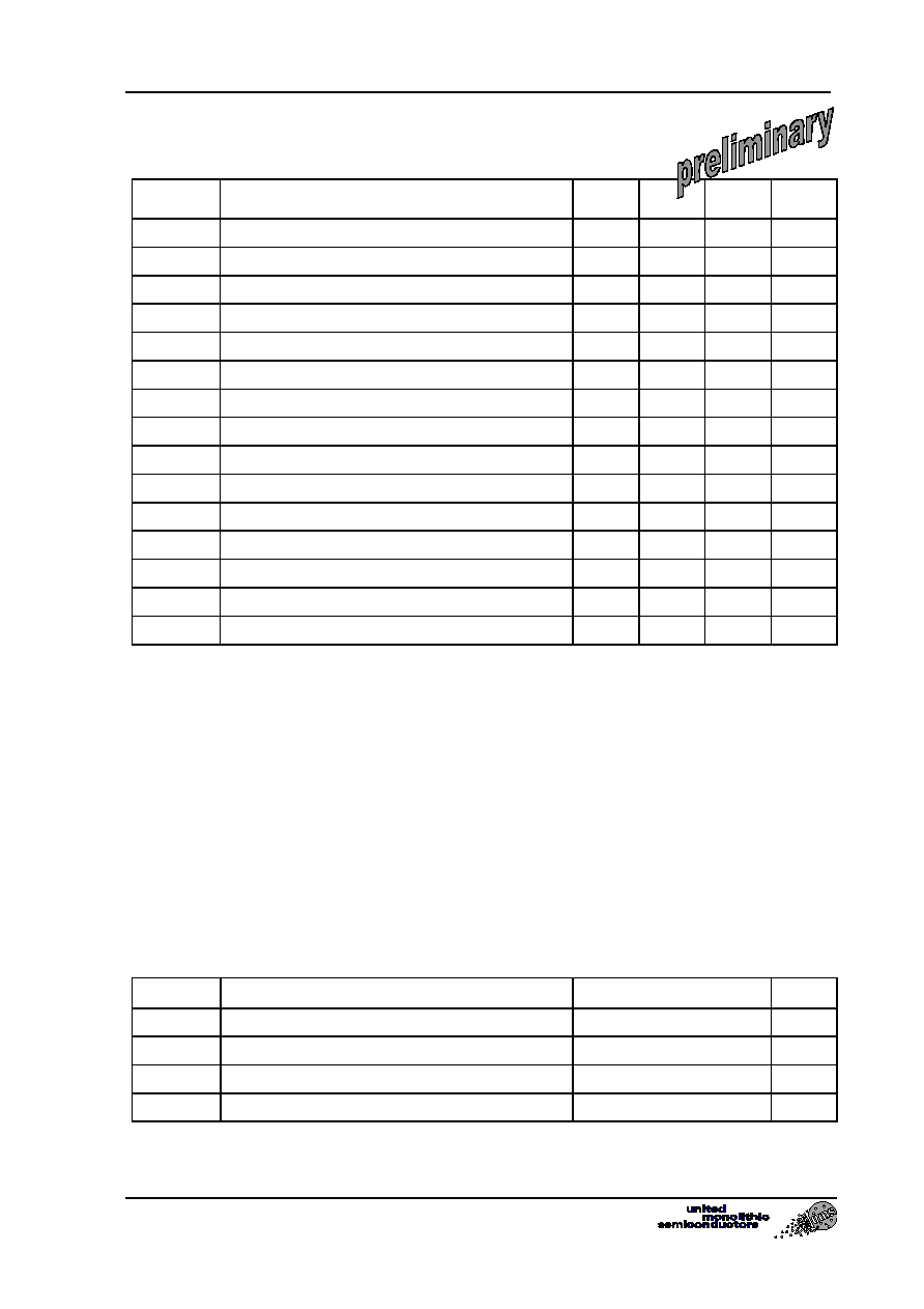
Main Characteristics
Tamb. = 25∞C
Parameter Min
Typ
Max
Unit
F
RF
RF frequency range
25
32
GHz
F
LO
LO frequency range
12
15.5
GHz
F
IF
IF frequency range
0.1
3
GHz
L
c
Conversion
Loss
11 15 dB
ESD Protection : Electrostatic discharge sensitive device. Observe handling precautions !
25-32GHz SSB Mixer
CHM1291
Ref. : DSCHM12912266 - 23-Sept.-02
2/6
Specifications subject to change without notice
Route DÈpartementale 128 , B.P.46 - 91401 ORSAY Cedex - FRANCE
Tel.: +33 (0)1 69 33 03 08 - Fax : +33 (0)1 69 33 03 09
Electrical Characteristics for Broadband Operation
Tamb = +25∞C, Vd = 3.5V Id=55mA
Symbol Parameter Min
Typ
Max
Unit
F
RF
RF frequency range
25
32
GHz
F
LO
LO frequency range
12
15.5
GHz
F
IF
IF frequency range
0.1
3
GHz
L
c
Conversion
Loss
11 15 dB
P
LO
LO Input power
+5
dBm
2xLO Leak 2xLO Leakage (for P
LO
=+5dBm)
-35
-30
dBm
Img Rej
Image Rejection (1)
10
15
dBc
P1dB
Input power at 1dB gain compression
-2
+1
dBm
P03
Input power at 3dB gain compression
+3
dBm
IP3 Input
3
rd
order intercept point
+9
dBm
LO Match LO VSWR
2.0:1
RF Match RF VSWR
2.0:1
IF Match IF VSWR
2.0:1
Sz
Chip
size
2.6 mm≤
Id Bias
current
55 mA
(1) With external quadrature hybrid coupler (reference on request). The minimal value depends
on the quality of the external quadrature combiner.
Current source biasing network is recommended.
A bonding wire of typically 0.1 to 0.15 nH will improve the accesses matching.
Absolute Maximum Ratings
Tamb. = 25∞C (1)
Symbol Parameter
Values
Unit
Vd Drain
bias
voltage
4.0
V
Id Drain
bias
current
100
mA
Ta
Operating temperature range
-40 to +85
∞C
Tstg
Storage temperature range
-55 to +155
∞C
(1) Operation of this device above anyone of these parameters may cause permanent damage.
(2) Duration < 1s.

25-32GHz SSB Mixer
CHM1291
Ref. : DSCHM12912266 - 23-Sept.-02
3/6
Specifications subject to change without notice
Route DÈpartementale 128 , B.P.46 - 91401 ORSAY Cedex - FRANCE
Tel.: +33 (0)1 69 33 03 08 - Fax : +33 (0)1 69 33 03 09
Typical On-wafer Measurements in Up-Conversion mode with
external IF quadrature combiner
Bias conditions: Tamb = +25∞C, Vd = 3.5V, Id = 55mA
Up-Conversion supradyne mode with external combiner
P LO = +5dBm F LO = 14GHz
-44
-40
-36
-32
-28
-24
-20
-16
-12
-8
-4
0
4
8
12
16
20
24
28
32
1,5
1,7
1,9
2,1
2,3
2,5
IF Frequency (GHz)
Conv
.
Los
s
(dB),
LO
& 2
x
L
O
leakag
e (
d
B
m
)
CL sup ( dB )
CL inf ( dB )
Img Supp ( dBc )
P LO @ RF ( dBm )
P 2xLO @ RF ( dBm )
Up-Conversion infradyne mode with external combiner
P LO = +5dBm F LO = 14GHz
-44
-40
-36
-32
-28
-24
-20
-16
-12
-8
-4
0
4
8
12
16
20
24
28
32
1,5
1,7
1,9
2,1
2,3
2,5
IF Frequency (GHz)
Conv
.
Los
s
(
d
B)
,
LO
& 2
x
L
O
l
eakag
e (d
B
m
)
CL sup ( dB )
CL inf ( dB )
Img Supp ( dBc )
P LO @ RF ( dBm )
P 2xLO @ RF ( dBm )
Up-Conversion supradyne mode with external combiner
P LO = +5dBm F IF = 2,0GHz
-54
-50
-46
-42
-38
-34
-30
-26
-22
-18
-14
-10
-6
-2
2
6
10
14
18
22
26
30
12
12,5
13
13,5
14
14,5
15
15,5
16
LO Frequency (GHz)
Conv
.
Los
s
(dB),
LO
& 2
x
L
O
leakag
e (
d
B
m
)
CL sup ( dB )
CL inf ( dB )
Img Supp (dBc)
P LO @ RF ( dBm )
P 2xLO @ RF ( dBm )
Up-Conversion infradyne mode with external combiner
P LO = +5dBm F IF = 2,0GHz
-54
-50
-46
-42
-38
-34
-30
-26
-22
-18
-14
-10
-6
-2
2
6
10
14
18
22
26
30
12
12,5
13
13,5
14
14,5
15
15,5
16
LO Frequency (GHz)
C
o
n
v
. L
o
ss (
d
B
)
, L
O
&
2xL
O
leakag
e (
d
B
m
)
CL sup ( dB )
CL inf ( dB )
Img Supp (dBc)
P LO @ RF ( dBm )
P 2xLO @ RF ( dBm )
Typical On-wafer Compression Measurements in Up-Conversion
mode with external IF quadrature combiner
Bias conditions: Tamb = +25∞C, Vd = 3.5V, Id = 55mA
Up-Conversion Sup. mode with external combiner
LO = 14GHz P LO = +5dBm F IF = 2,0GHz (RF = 30GHz)
-30
-28
-26
-24
-22
-20
-18
-16
-14
-12
-10
-8
-6
-4
-2
-20
-18
-16
-14
-12
-10
-8
-6
-4
-2
0
2
4
6
IF Input power (dBm)
O
u
tput pow
e
r
& Conv
.
Los
s
(dBm
& dB)
P RF 30GHz
CL 30GHz
Up-Conversion Inf. mode with external combiner
LO = 14GHz P LO = +5dBm F IF = 2,0GHz (RF = 26GHz)
-30
-28
-26
-24
-22
-20
-18
-16
-14
-12
-10
-8
-6
-4
-2
-20
-18
-16
-14
-12
-10
-8
-6
-4
-2
0
2
4
6
IF Input power (dBm)
O
u
tput pow
e
r
& Conv
.
Los
s
(dBm
& dB)
P RF 26GHz
CG 26GHz

25-32GHz SSB Mixer
CHM1291
Ref. : DSCHM12912266 - 23-Sept.-02
4/6
Specifications subject to change without notice
Route DÈpartementale 128 , B.P.46 - 91401 ORSAY Cedex - FRANCE
Tel.: +33 (0)1 69 33 03 08 - Fax : +33 (0)1 69 33 03 09
Typical On-wafer Measurements in Down-Conversion mode with
external IF quadrature combiner
Bias conditions: Tamb = +25∞C, Vd = 3.5V, Id = 55mA
Down-Conversion mode with external combiner
P LO = +5dBm F LO = 12GHz
-34
-32
-30
-28
-26
-24
-22
-20
-18
-16
-14
-12
-10
-8
-6
21,5
22,0
22,5
23,0
23,5
24,0
24,5
25,0
25,5
26,0
26,5
RF Frequency (GHz)
C
o
n
ver
si
o
n
L
o
ss (d
B
)
CL I Sup ( dB )
CL I Inf ( dB )
CL Q Sup ( dB )
CL Q Inf ( dB )
F LO
Down-Conversion mode with external combiner
P LO = +5dBm F LO = 14GHz
-34
-32
-30
-28
-26
-24
-22
-20
-18
-16
-14
-12
-10
-8
-6
25,5
26,0
26,5
27,0
27,5
28,0
28,5
29,0
29,5
30,0
30,5
RF Frequency (GHz)
Co
n
versi
o
n
L
o
ss (
d
B)
CL I Sup ( dB )
CL I Inf ( dB )
CL Q Sup ( dB )
CL Q Inf ( dB )
F LO
Down-Conversion mode with external combiner
P LO = +5dBm F LO = 16GHz
-34
-32
-30
-28
-26
-24
-22
-20
-18
-16
-14
-12
-10
-8
-6
29,5
30,0
30,5
31,0
31,5
32,0
32,5
33,0
33,5
34,0
34,5
RF Frequency (GHz)
Co
n
versi
o
n
L
o
ss (
d
B)
CL I Sup ( dB )
CL I Inf ( dB )
CL Q Sup ( dB )
CL Q Inf ( dB )
F LO
Down-Conversion mode with external combiner
P LO = +5dBm F IF = 2,0GHz
-54
-50
-46
-42
-38
-34
-30
-26
-22
-18
-14
-10
-6
12
12,5
13
13,5
14
14,5
15
15,5
16
LO Frequency (GHz)
C
o
n
v
. L
o
ss (
d
B
)
, L
O
&
2xL
O
leakag
e (
d
B
m
)
CL I Sup ( dB )
CL I Inf ( dB )
CL Q Sup ( dB )
CL Q Inf ( dB )
P LO @ RF ( dBm )
P 2xLO ( dBm )
Typical On-wafer Measurements in Down-Conversion mode without
external IF quadrature combiner
Bias conditions: Tamb = +25∞C, Vd = 3.5V, Id = 55mA
Down-Conversion Sup. mode without external combiner
F LO = 13GHz P LO = +5dBm F RF = 26 to 33GHz
-58
-54
-50
-46
-42
-38
-34
-30
-26
-22
-18
-14
-10
0
1
2
3
4
5
6
7
IF Frequency (GHz)
C
onv
. Los
s
(
d
B
)
L
O
& 2L
O
l
eakag
e (
d
Bm)
CL I Sup ( dB )
CL Q Sup ( dB )
P LO @ IF ( dBm )
P 2XLO @ IF ( dBm )
Down-Conversion Inf. mode without external combiner
F LO = 15GHz P LO = +5dBm F RF = 23 to 29GHz
-58
-54
-50
-46
-42
-38
-34
-30
-26
-22
-18
-14
-10
0
1
2
3
4
5
6
7
IF Frequency (GHz)
C
onv
. Los
s
(
d
B
)
L
O
& 2L
O
l
eakag
e (
d
Bm)
CL I Inf ( dB )
CL Q Inf ( dB )
P LO @ IF ( dBm )
P 2XLO @ IF ( dBm )

25-32GHz SSB Mixer
CHM1291
Ref. : DSCHM12912266 - 23-Sept.-02
5/6
Specifications subject to change without notice
Route DÈpartementale 128 , B.P.46 - 91401 ORSAY Cedex - FRANCE
Tel.: +33 (0)1 69 33 03 08 - Fax : +33 (0)1 69 33 03 09
Chip Assembly and Mechanical Data
Note : Supply feed should be capacitively bypassed. 25µm diameter gold wire is recommended
Bonding pad positions
( Chip thickness : 100µm. All dimensions are in micrometers )