 | –≠–ª–µ–∫—Ç—Ä–æ–Ω–Ω—ã–π –∫–æ–º–ø–æ–Ω–µ–Ω—Ç: CHM2179A | –°–∫–∞—á–∞—Ç—å:  PDF PDF  ZIP ZIP |
CHM2179a
Ref. : DSCH21790192 - 22-Jun-00
1/6
Specifications subject to change without notice
United Monolithic Semiconductors S.A.S.
Route DÈpartementale 128 - B.P.46 - 91401 Orsay Cedex France
Tel. : +33 (0)1 69 33 03 08 - Fax : +33 (0)1 69 33 03 09
W-band Mixer
GaAs Monolithic Microwave IC
Description
The CHM2179a is a balanced Schottky
diode mixer based on a six quarter wave
ring structure. This circuit is manufactured
with the BES-MMIC process: 1 µm
Schottky diode device, air bridges, via
holes through the substrate, stepper
lithography.
It is available in chip form.
Main Features
W-band LO and RF frequency range
Low conversion loss
IF from DC to 100MHz
High LO/RF isolation
High LO/AM noise rejection
Very low IF noise
Low LO input power
Small chip size: 1.53 x 1.17 x 0.10 mm
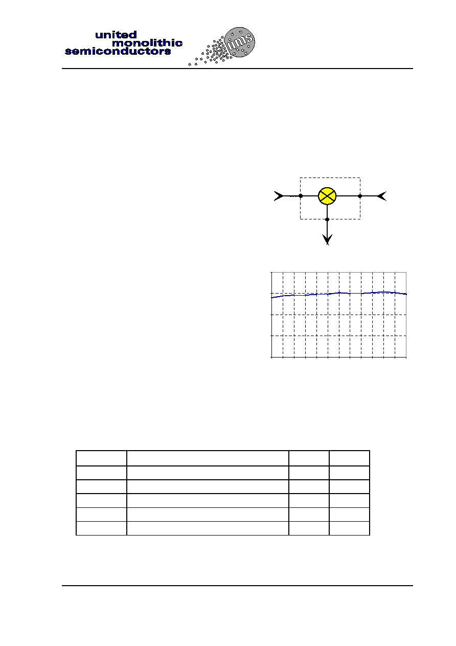
RF
IF
LO
-15
-12,5
-10
-7,5
-5
75
75,5
76
76,5
77
77,5
78
LO Frequency (GHz)
C
o
n
ver
si
o
n
l
o
ss (
d
B
)
Typical conversion characteristic
LO power = 5dBm ; IF=10MHz
(measurement in test fixture)
Main Characteristics
Tamb. = 25∞C
Symbol
Parameter
Typ
Unit
F_LO,F_RF LO,RF frequency range
76-77
GHz
F_IF
IF frequency range
DC-100
MHz
Lc
Conversion loss
7.5
dB
I_LO/RF
LO/RF isolation
20
dB
N_IF
IF noise density @ 100kHz
-158
dBm/Hz
ESD Protection : Electrostatic discharge sensitive device. Observe handling precautions !
CHM2179a
W-band Mixer
Ref. : DSCH21790192 - 22-Jun-00
2/6
Specifications subject to change without notice
Route DÈpartementale 128 , B.P.46 - 91401 ORSAY Cedex - FRANCE
Tel.: +33 (0)1 69 33 03 08 - Fax : +33 (0)1 69 33 03 09
Electrical Characteristics
Tamb. = 25∞C, used according to section "Typical bias and IF configuration" and "Typical
assembly and RF configuration"
Symbol
Parameter
Min
Typ
Max
Unit
F_LO,F_RF
LO,RF frequency range
76-77
GHz
F_IF
IF frequency range
DC-100
MHz
Lc
Conversion loss
7.5
9
dB
P_LO
LO input power
3
5
7
dBm
VSWR_LO
LO port VSWR (50
)
2:1
VSWR_RF
RF port VSWR (50
)
2:1
IF_load
IF load impedance
200
I_LO/RF
LO/RF isolation
17
22
dB
R_AM_LO
LO AM noise rejection
27
dB
N_IF
IF noise density @ 100kHz (1)
-158
dBm/Hz
Id
Supply current (2)
1
mA
(1) Measured on 50
IF load impedance.
(2) See on chapter "Typical bias and IF configuration"
Absolute Maximum Ratings (1)
Tamb = +25∞C
Symbol
Parameter
Values
Unit
Id
Supply current
3
mA
P_LO
Maximum peak input power overdrive at LO port (2)
10
dBm
P_RF
Maximum peak input power overdrive at RF port (2)
10
dBm
Top
Operating temperature range
-40 to +100
∞C
Tstg
Storage temperature range
-55 to +125
∞C
(1) Operation of this device above anyone of these parameters may cause permanent damage.
(2) Duration < 1s

W-band Mixer
CHM2179a
Ref. : DSCH21790192 - 22-Jun-00
3/6
Specifications subject to change without notice
Route DÈpartementale 128 , B.P.46 - 91401 ORSAY Cedex - FRANCE
Tel.: +33 (0)1 69 33 03 08 - Fax : +33 (0)1 69 33 03 09
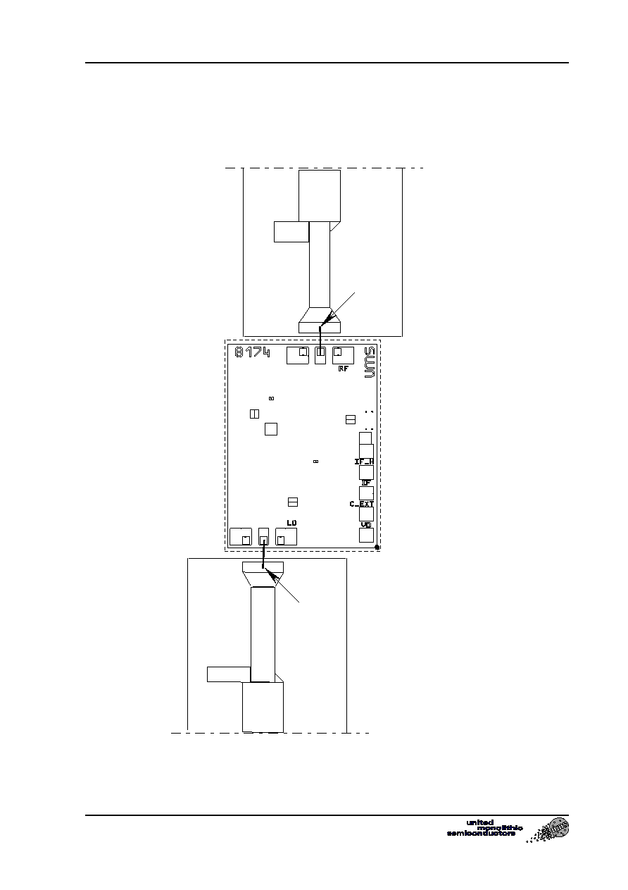
Chip Mechanical Data and Pin References
1
2
3
4
5
6
7
8
9
11
10
Unit = µm
External chip size = 1530 x 1170
Chip thickness = 100 +/- 10
HF Pads (2,5) = 68 x 118
DC/IF Pads = 100 x 100
Pin number
Pin name
Description
1,3,4,6
Ground : should not be bonded. If required,
please ask for more information.
2
LO
LO input
5
RF
RF input
7
GND
Ground (optional)
8
Not Connected
9
IF
IF output
10
C_ext
Bias decoupling
11
+V
Positive supply voltage

CHM2179a
W-band Mixer
Ref. : DSCH21790192 - 22-Jun-00
4/6
Specifications subject to change without notice
Route DÈpartementale 128 , B.P.46 - 91401 ORSAY Cedex - FRANCE
Tel.: +33 (0)1 69 33 03 08 - Fax : +33 (0)1 69 33 03 09
Typical Bias and IF Configuration
Several external configurations are possible for bias and IF. The objective is to give
flexibility for the integration.
As this component is mainly dedicated to low IF use, there are several possibilities for
interfacing with low noise IF amplifier. The optimum IF load for conversion loss is 200
,
however depending on the IF amplifier noise characteristic this load can be modified in order
to optimise the noise figure. A series capacitor, between IF output and the load is
recommended.
Due to high sensitivity to electrical discharges a integrated resistance is used and two ports
are available for biasing. One is for the connection of a decoupling capacitor (C_ext) and the
other one is for the supply voltage connection through an external series resistance (+V
port). However, in order to keep the compatibility with the CHM2179, only the "C_ext" port
can be used.
RF
LO
+V
1k
IF
+V
C_ext
R_bias1
R_load_IF
C_IF
C_bias
Recommended external bias and
IFconfiguration
RF
LO
+V
1k
IF
+V
C_ext
R_bias2
R_load_IF
C_IF
C_bias
Other possible configuration
(compatible with the previous version)
The recommended values for external components are:
C_bias
R_bias*C >> 1/F_IF
R_bias1
2.9k
for 1mA current consumption (V = 4.5V, typical LO
power)
R_bias2
R_bias2 = R_bias1 + 1k
R_load_IF
From 50 to 200
Notes::
1. R_bias = R_bias1 + 1k
when "+V" port is used, otherwize R_bias = R_bias2
2. R_bias can be adjusted if necessary; This allows to optimise the performances when
some parameters are different from recommended ones (Supply voltage, LO power ...).
However maximum ratings for the current have to be taken into account.
3. A series capacitor at IF outputs is recommended for DC decoupling.
W-band Mixer
CHM2179a
Ref. : DSCH21790192 - 22-Jun-00
5/6
Specifications subject to change without notice
Route DÈpartementale 128 , B.P.46 - 91401 ORSAY Cedex - FRANCE
Tel.: +33 (0)1 69 33 03 08 - Fax : +33 (0)1 69 33 03 09
Typical Assembly and RF Configuration
In order to use acceptable wire bonding length, compatible with automatic
pick and place and wire bonding equipment, an external matching network is
proposed on low dielectric constant substrate.
L
~
0
.
2
5
n
H
E
r
~
2
.
2
h
=
0
.
1
2
7
m
m
L
~
0
.
2
5
n
H
E
r
~
2
.
2
h
=
0
.
1
2
7
m
m
50 Ohm
50 Ohm
1
0
0
1
2
0
6
3
0
2
0
0
3
2
0
390
200
390
1
0
0
1
2
0
8
6
0
1
5
0
4
2
0
390
250
390
1
2
3
4
5
6
7
8
9
1
1
1
0
Example of integration using low dielectric constant substrate : Er=2.2,
heigh=0.127mm (dimensions are in µm)