CHP6013-SRF
Ref. : DSCHP60133112 - 22 Apr 03
1/5
Specifications subject to change without notice
United Monolithic Semiconductors S.A.S.
Route Départementale 128 - B.P.46 - 91401 Orsay Cedex France
Tel. : +33 (0)1 69 33 03 08 - Fax : +33 (0)1 69 33 03 09
L-band Phase Shifter
GaAs Monolithic Microwave IC
in surface mount ceramic-metal package
Description
The CHP6013 is a L-band monolithic 6-bit
phase shifter.
The circuit is manufactured with a
standard 0.7µm MESFET process : via
holes through the substrate, air bridges
and electron beam gate lithography. It is
supplied in surface mount ceramic-metal
package
Main Features
Frequency range : 1.2 to 1.4GHz
5.625° phase step
64 states
0/-6V control voltage
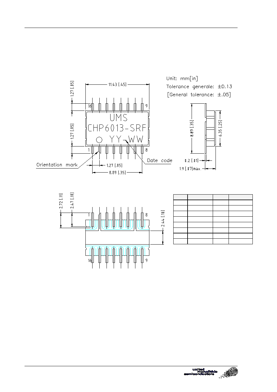
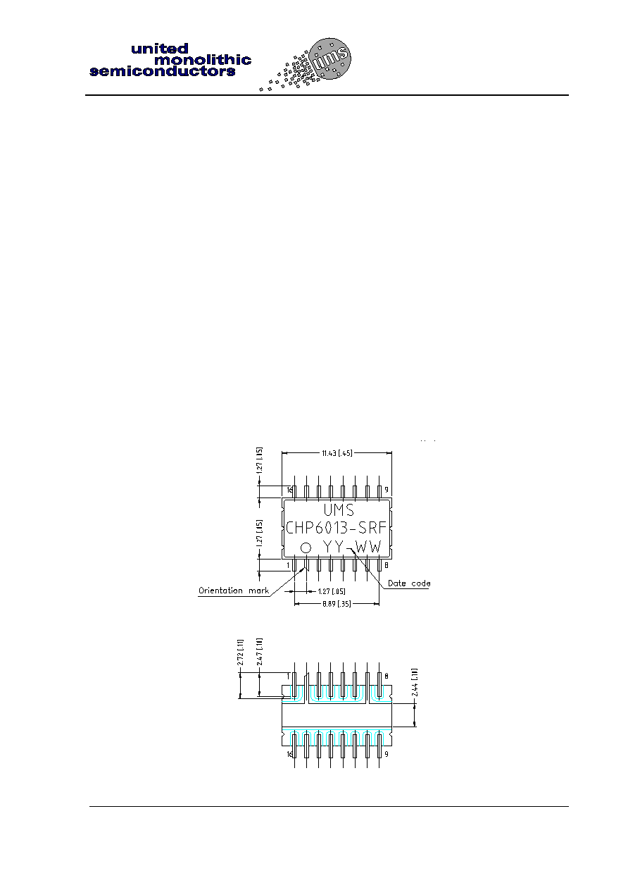
Surface mount package
dimension: 11.43 x 8.89 x 1.9 mm
3
Surface mount ceramic-metal package :
CHP6013-SRF
L-band Phase Shifter
Ref. : DSCHP60133112 - 22 Apr 03
2/5
Specifications subject to change without notice
Route Départementale 128 , B.P.46 - 91401 ORSAY Cedex - FRANCE
Tel.: +33 (0)1 69 33 03 08 - Fax : +33 (0)1 69 33 03 09
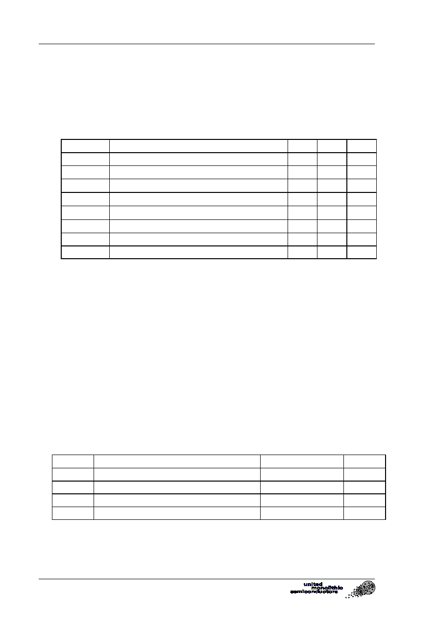
Electrical Characteristics
·
Tamb = +25°C
·
Test conditions: Pin
0dBm, Low level control voltage = -6V, High level control voltage = 0V
·
Specifications for the main bit states: 0, 1, 2, 4, 8, 16, 32 and 63
Symbol Parameter Min
Max
Unit
Fop
Operating frequency range
1.2
1.4
GHz
AV Amplitude
variation
±
0.7
dB
PPE
Peak Phase Error
±
5
°
IL
Insertion loss
8.5
dB
IL
m
Insertion loss match at state 0 unit to unit
(1)
±
0.25
dB
Ipm
Insertion phase match at state 0 unit to unit
(1)
±
7
°
VSWRin
Input
VSWR
2:1
VSWRout
Ouput
VSWR
2:1
(1) Average value defined by production lot.
ESD Protections : Electrostatic discharge sensitive device observe handling precautions !
Peak Phase Error (PPE) definition:
PPE(i)=measured_phase(S21)@state(i) measured_phase(S21)@state(0) theoretical_phase
value@state(i)
(i) = 0, 1, 2, 4, 8, 16, 32, 63 = main bit states.
Amplitude variation (AV) definition:
AV(i) = measured_dB(S21)@state(i) measured_dB(S21)@state(0)
(i) = 0, 1, 2, 4, 8, 16, 32, 63 = main bit states.
Absolute Maximum Ratings
Tamb = +25°C
Operation of this device above anyone of these paramaters may cause permanent damage.
Symbol Parameter
Values
Unit
Vgi
Phase shifter control voltage
-7.5
V
Pin
Maximum peak input power overdrive (1)
+30
dBm
Top
Operating temperature range
-40 to +85
°C
Tstg
Storage temperature range
-55 to +125
°C
(1) Duration < 1s.
L-band Phase Shifter
CHP6013-SRF
Ref. : DSCHP60133112 - 22 Apr 03
3/5
Specifications subject to change without notice
Route Départementale 128 , B.P.46 - 91401 ORSAY Cedex - FRANCE
Tel.: +33 (0)1 69 33 03 08 - Fax : +33 (0)1 69 33 03 09
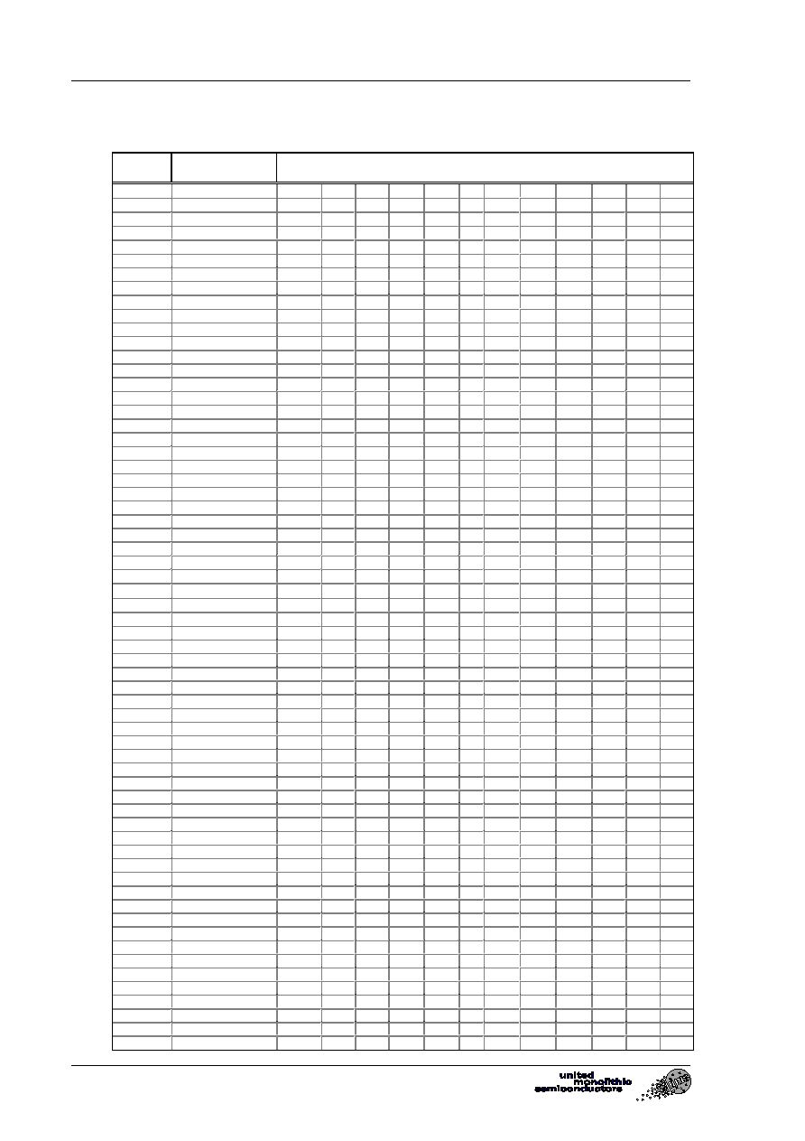
Phase Shifter Control Interface
The 6-bit phase shifter command is actuated by 12 voltage control leads.
BIT Theoretical
Control voltages (V)
STATE
phase state (°)
B18 B90 B45 B22 B11 B5
H18 H90 H45 H22 H11 H5
0 0
0 0 0 0 0
0
-6
-6
-6
-6
-6
-6
1 5,625
0 0 0 0 0
-6
-6
-6
-6
-6
-6
0
2 11,25
0 0 0 0 -6
0
-6
-6
-6
-6
0
-6
3
16,875
0 0 0 0 -6
-6
-6 -6 -6 -6 0 0
4 22,5
0 0 0
-6 0
0
-6
-6
-6 0
-6
-6
5 28,125
0
0
0
-6
0
-6
-6
-6
-6
0
-6
0
6 33,75
0
0
0
-6
-6
0
-6
-6
-6
0
0
-6
7
39,375
0 0 0 -6 -6
-6
-6 -6 -6 0 0 0
8 45
0 0
-6
0 0
0
-6
-6 0 -6
-6
-6
9 50,625
0
0
-6
0
0
-6
-6
-6
0
-6
-6
0
10 56,25 0
0
-6
0
-6
0
-6
-6
0
-6
0
-6
11 61,875 0
0
-6
0
-6
-6
-6
-6
0
-6
0
0
12 67,5 0
0
-6
-6
0
0
-6
-6
0
0
-6
-6
13 73,125 0
0
-6
-6
0
-6
-6
-6
0
0
-6
0
14 78,75 0
0
-6
-6
-6
0
-6
-6
0
0
0
-6
15 84,375 0
0
-6
-6
-6
-6
-6
-6
0
0
0
0
16 90 0 -6 0 0 0
0
-6 0 -6 -6
-6
-6
17 95,625 0
-6
0
0
0
-6
-6
0
-6
-6
-6
0
18 101,25 0
-6
0
0
-6
0
-6
0
-6
-6
0
-6
19 106,875 0
-6
0
0
-6
-6
-6
0
-6
-6
0
0
20 112,5 0
-6
0
-6
0
0
-6
0
-6
0
-6
-6
21 118,125 0
-6
0
-6
0
-6
-6
0
-6
0
-6
0
22 123,75 0
-6
0
-6
-6
0
-6
0
-6
0
0
-6
23 129,375 0
-6
0
-6
-6
-6
-6
0
-6
0
0
0
24
135
0 -6 -6 0 0 0 -6 0 0 -6 -6 -6
25 140,625 0
-6
-6
0
0
-6
-6
0
0
-6
-6
0
26 146,25 0
-6
-6
0
-6
0
-6
0
0
-6
0
-6
27 151,875 0
-6
-6
0
-6
-6
-6
0
0
-6
0
0
28
157,5
0 -6 -6 -6 0 0 -6 0 0 0 -6 -6
30 168,75 0
-6
-6
-6
-6
0
-6
0
0
0
0
-6
31 174,375 0
-6
-6
-6
-6
-6
-6
0
0
0
0
0
32 180 -6 0 0 0 0
0
0 -6 -6 -6
-6
-6
33 185,625 -6
0
0
0
0
-6
0
-6
-6
-6
-6
0
34 191,25 -6
0
0
0
-6
0
0
-6
-6
-6
0
-6
35
196,875
-6 0 0 0 -6
-6 0 -6 -6 -6 0 0
36 202,5 -6
0
0
-6
0
0
0
-6
-6
0
-6
-6
37 208,125 -6
0
0
-6
0
-6
0
-6
-6
0
-6
0
38 213,75 -6
0
0
-6
-6
0
0
-6
-6
0
0
-6
39
219,375
-6 0 0 -6 -6
-6 0 -6 -6 0 0 0
40 225 -6
0
-6
0
0
0
0
-6
0
-6
-6
-6
41 230,625 -6
0
-6
0
0
-6
0
-6
0
-6
-6
0
42 236,25 -6
0
-6
0
-6
0
0
-6
0
-6
0
-6
43 241,875 -6
0
-6
0
-6
-6
0
-6
0
-6
0
0
44 247,5 -6
0
-6
-6
0
0
0
-6
0
0
-6
-6
45 253,125 -6
0
-6
-6
0
-6
0
-6
0
0
-6
0
46 258,75 -6
0
-6
-6
-6
0
0
-6
0
0
0
-6
47 264,375 -6
0
-6
-6
-6
-6
0
-6
0
0
0
0
48 270 -6
-6
0
0
0
0
0
0
-6
-6
-6
-6
49 275,625 -6
-6
0
0
0
-6
0
0
-6
-6
-6
0
50 281,25 -6
-6
0
0
-6
0
0
0
-6
-6
0
-6
51 286,875 -6
-6
0
0
-6
-6
0
0
-6
-6
0
0
52 292,5 -6
-6
0
-6
0
0
0
0
-6
0
-6
-6
53 298,125 -6
-6
0
-6
0
-6
0
0
-6
0
-6
0
54 303,75 -6
-6
0
-6
-6
0
0
0
-6
0
0
-6
55 309,375 -6
-6
0
-6
-6
-6
0
0
-6
0
0
0
56
315
-6 -6 -6 0 0 0 0 0 0 -6 -6 -6
57 320,625 -6
-6
-6
0
0
-6
0
0
0
-6
-6
0
58 326,25 -6
-6
-6
0
-6
0
0
0
0
-6
0
-6
59 331,875 -6
-6
-6
0
-6
-6
0
0
0
-6
0
0
60
337,5
-6 -6 -6 -6 0 0 0 0 0 0 -6 -6
61 343,125 -6
-6
-6
-6
0
-6
0
0
0
0
-6
0
62 348,75 -6
-6
-6
-6
-6
0
0
0
0
0
0
-6
63 354,375 -6 -6 -6 -6 -6
-6
0 0 0 0 0 0
L-band Phase Shifter
CHP6013-SRF
Ref. : DSCHP60133112 - 22 Apr 03
5/5
Specifications subject to change without notice
Route Départementale 128 , B.P.46 - 91401 ORSAY Cedex - FRANCE
Tel.: +33 (0)1 69 33 03 08 - Fax : +33 (0)1 69 33 03 09
Ordering Information
Package form : CHP6013-SRF/23
Information furnished is believed to be accurate and reliable. However, United Monolithic Semiconductors S.A.S.
assumes no responsibility for the consequences of use of such information nor for any infringement of patents or other
rights of third parties, which may result from its use. No license is granted by implication or otherwise under any patent
or patent rights of United Monolithic Semiconductors S.A.S.. Specifications mentioned in this publication are subject
to change without notice. This publication supersedes and replaces all information previously supplied. United
Monolithic Semiconductors S.A.S. products are not authorised for use as critical components in life support devices
or systems without express written approval from United Monolithic Semiconductors S.A.S.