CHR2295
Ref. : DSCHR22951201 -20-July-01
1/6
Specifications subject to change without notice
Route DÈpartementale 128 , B.P.46 - 91401 ORSAY Cedex - FRANCE
Tel.: +33 (0)1 69 33 03 08 - Fax : +33 (0)1 69 33 03 09
24-30GHz Integrated Down Converter
GaAs Monolithic Microwave IC
Description
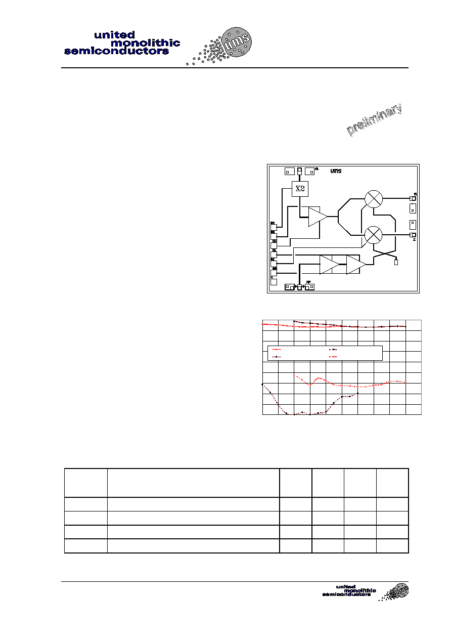
The CHR2295 is a multifunction chip which
integrates a LO time two multiplier, a balanced
cold FET mixer, and a RF LNA. It is designed for
a wide range of applications, typically commercial
communication systems. The backside of the
chip is both RF and DC grounds. This helps
simplify the assembly process.
The circuit is manufactured with a PM-HEMT
process, 0.25µm gate length, via holes through
the substrate, air bridges and electron beam
gate lithography.
It is available in chip form.
Main Features
∑
Broadband performances : 24-30GHz
∑
11 dB conversion gain
∑
3.5.0dB noise figure
∑
10dBm LO input power
∑
-10dBm RF input power (1dB gain comp.)
∑
Low DC power consumption, 120mA@3.5V
∑
Chip size : 2.49 X 1.97 X 0.10 mm
-24.00
-20.00
-16.00
-12.00
-8.00
-4.00
0.00
4.00
8.00
12.00
22.5
23.5
24.5
25.5
26.5
27.5
28.5
29.5
30.5
31.5
32.5
2XLO Frequency (GHz)
(d
B
)
Gc_channel_sup_rf+
Gc_channel_inf_rf+
Gc_channel inf_rf-
Gc_channel_sup_rf-
Conversion Gain & Image suppression @ IF=1.5GHz
(including test board losses)
Main Characteristics
Tamb. = 25∞C
Parameter Min
Typ
Max
Unit
F
RF
RF frequency range
24
30
GHz
F
LO
LO frequency range
12
15
GHz
F
IF
IF frequency range
0.25
1.5
GHz
G
c
Conversion
gain
11 dB
ESD Protection : Electrostatic discharge sensitive device. Observe handling precautions !
LO
Q
I
GM
GB
VDM
VDL
GX
VGA
RF
24-30GHz MFC Down Converter
CHR2295
Ref. : : DSCHR22951201 -20-July-01
2/6
Specifications subject to change without notice
Route DÈpartementale 128 , B.P.46 - 91401 ORSAY Cedex - FRANCE
Tel.: +33 (0)1 69 33 03 08 - Fax : +33 (0)1 69 33 03 09
Electrical Characteristics for Broadband Operation
Tamb = +25∞C, Vd = 3.5V
Symbol Parameter Min
Typ
Max
Unit
F
RF
RF frequency range
24
30
GHz
F
LO
LO frequency range
12
15
GHz
F
IF
IF frequency range
0.25
1.5
GHz
G
c
Conversion gain (1)
11
dB
NF
Noise
Figure
3.5 dB
P
LO
LO Input power
+10
dBm
Img Sup Image Suppression
17
dBc
P1dB
Input power at 1dB gain compression
-10
dBm
LO VSWR Input LO VSWR (1)
2.0:1
RF VSWR Input RF VSWR (1)
3.0:1
Id
Bias current (2)
120
mA
(1) On
Wafer
measurements
(2) Current source biasing network is recommended. Optimum performances for Idm= 50mA
and Idl= 70mA
Absolute Maximum Ratings
Tamb. = 25∞C (1)
Symbol Parameter
Values
Unit
Vd Drain
bias
voltage
4.0
V
Id Drain
bias
current
200
mA
Vg
Gate bias voltage
-2.0 to +0.4
V
Pin
Maximum peak input power overdrive (2)
+15
dBm
Ta
Operating temperature range
-40 to +85
∞C
Tstg
Storage temperature range
-55 to +155
∞C
(1) Operation of this device above anyone of these parameters may cause permanent damage.
(2) Duration < 1s.
24-30GHz MFC Down Converter
CHR2295
Ref. : : DSCHR22951201 -20-July-01
3/6
Specifications subject to change without notice
Route DÈpartementale 128 , B.P.46 - 91401 ORSAY Cedex - FRANCE
Tel.: +33 (0)1 69 33 03 08 - Fax : +33 (0)1 69 33 03 09
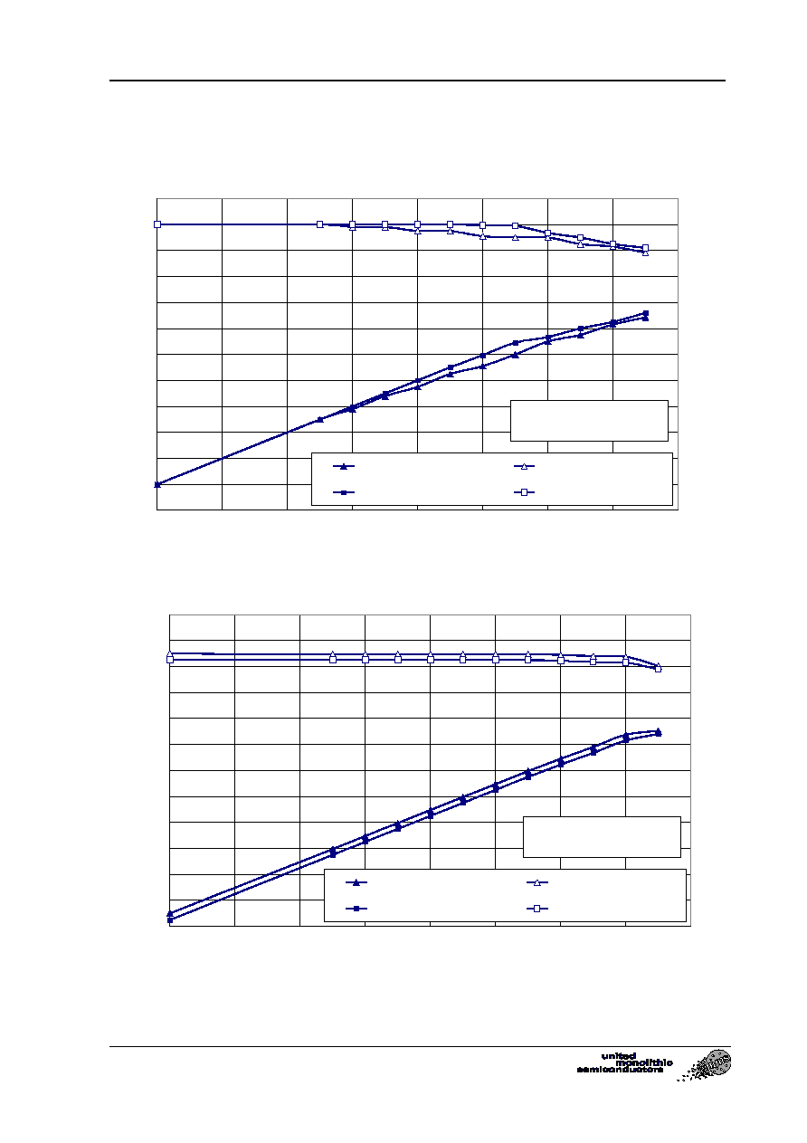
Typical On-wafer Measurements
Bias Conditions : Vdm= Vdl= 3.5 V, Vgm= -0.9V, Vgb= -0.3V, Vgx= -0.7V, Vga= -0.2V
-14
-12
-10
-8
-6
-4
-2
0
2
4
6
8
10
-20
-18
-16
-14
-12
-10
-8
-6
-4
Input RF power (dBm)
IF power_I (dBm)
Conv_gain I (dB)
IF power_Q (dBm)
Conv_gain Q (dB)
Freq_RF= 24.6GHz
Freq_LO= 12.05GHz
-14
-12
-10
-8
-6
-4
-2
0
2
4
6
8
10
-20
-18
-16
-14
-12
-10
-8
-6
-4
Input RF power (dBm)
IF power_I (dBm)
Conv_gain I (dB)
IF power_Q (dBm)
Conv_gain Q (dB)
Freq_RF= 28GHz
Freq_LO= 13.75GHz
Input RF compression by channel

24-30GHz MFC Down Converter
CHR2295
Ref. : : DSCHR22951201 -20-July-01
4/6
Specifications subject to change without notice
Route DÈpartementale 128 , B.P.46 - 91401 ORSAY Cedex - FRANCE
Tel.: +33 (0)1 69 33 03 08 - Fax : +33 (0)1 69 33 03 09
Typical On-board Measurements
Bias Conditions : Vdm= Vdl= 3.5 V, Vgm= Vgx= -0.9V, Vgb= Vga= -0.3V
All these measurements include the losses from the test board (about 1dB on the conversion
gain and 0.5dB on the noise figure).
-24.00
-20.00
-16.00
-12.00
-8.00
-4.00
0.00
4.00
8.00
12.00
22.5
23.5
24.5
25.5
26.5
27.5
28.5
29.5
30.5
31.5
32.5
2XLO Frequency (GHz)
Con
v
er
s
i
on Gai
n
& Image suppr
es
si
on (
d
B)
IF=1GHz
IF=1.5GHz
IF=2GHz
IF=1GHz
IF=1.5GHz
IF=2GHz
Conversion gain & Image suppression versus IF frequency
0
1
2
3
4
5
6
7
8
9
10
24.5
25
25.5
26
26.5
27
27.5
28
28.5
29
29.5
RF Frequency (GHz)
N
o
i
s
e factor
(
d
B)
Channel_sup_IF_1GHz
Channel_inf_IF_1GHz
Channel_sup_IF_1.5GHz
Channel_inf_IF_1.5GHz
Channel_sup_IF_2GHz
Channel_inf_IF_2GHz
Noise figure supradyne & infradyne versus IF frequency
24-30GHz MFC Down Converter
CHR2295
Ref. : : DSCHR22951201 -20-July-01
5/6
Specifications subject to change without notice
Route DÈpartementale 128 , B.P.46 - 91401 ORSAY Cedex - FRANCE
Tel.: +33 (0)1 69 33 03 08 - Fax : +33 (0)1 69 33 03 09
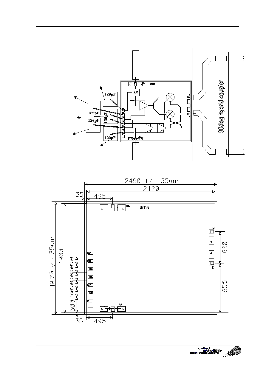
Chip Assembly and Mechanical Data
LO
IN
RF
IN
Q
OUT
I
OUT
To Vgm DC Gate Supply
To Vgb DC Gate Supply
To Vgx DC Gate Supply
To Vga DC Gate Supply
To Vdm,Vdl DC Drain Supply
Note : Supply feed should be capacitively bypassed. 25µm diameter gold wire is recommended
Bonding pad positions
( Chip thickness : 100µm. All dimensions are in micrometers )