
CHR2296
Ref. : DSCHR22962147 25-May-02
1/5
Specifications subject to change without notice
Route DÈpartementale 128 , B.P.46 - 91401 ORSAY Cedex - FRANCE
Tel.: +33 (0)1 69 33 03 08 - Fax : +33 (0)1 69 33 03 09
36- 40GHz Integrated Down Converter
GaAs Monolithic Microwave IC
Description
The CHR2296 is a multifunction chip which
integrates a LO time two multiplier, a balanced
cold FET mixer, and a RF LNA. It is designed for
a wide range of applications, typically commercial
communication systems. The backside of the
chip is both RF and DC grounds. This helps
simplify the assembly process.
The circuit is manufactured with a PM-HEMT
process, 0.25µm gate length, via holes through
the substrate, air bridges and electron beam
gate lithography.
It is available in chip form.
Main Features
∑
Broadband performances : 36-40GHz
∑
11 dB conversion gain
∑
5dB noise figure
∑
10dBm LO input power
∑
-10dBm RF input power (1dB gain comp.)
∑
Low DC power consumption, 110mA@3.5V
∑
Chip size : 2.49 X 1.97 X 0.10 mm
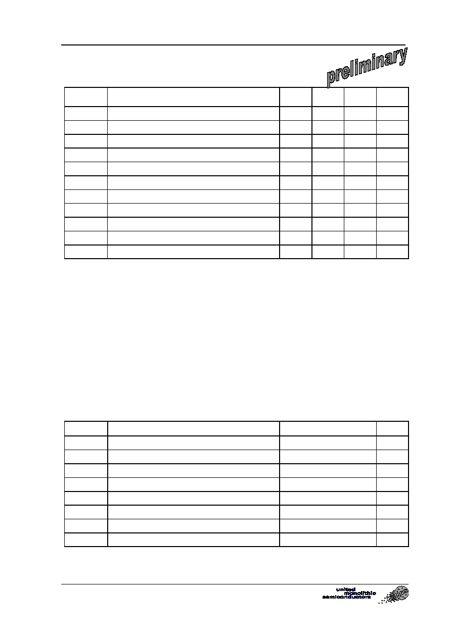
Typical on wafer measurement:
Conversion Gain & Image suppression @ IF=1GHz
Main Characteristics
Tamb. = 25∞C
Parameter Min
Typ
Max
Unit
F
RF
RF frequency range
36
40
GHz
F
LO
LO frequency range
17
20
GHz
F
IF
IF frequency range
0.25
1.5
GHz
G
c
Conversion
gain
11 dB
ESD Protection : Electrostatic discharge sensitive device. Observe handling precautions !
LO
Q
I
GM
GB
VDM
VDL
GX
VGA
RF
-28
-24
-20
-16
-12
-8
-4
0
4
8
12
16
34
35
36
37
38
39
40
2*LO Frequency (GHz)
C
onver
si
on G
a
i
n
& I
m
age suppr
essi
on (
d
B)
Gc_channel_inf_rf-
Gc_channel_sup_rf-
Gc_channel_inf_rf+
Gc_channel_sup_rf+
36-40 MFC Down Converter
CHR2296
Ref. : DSCHR22962147 25-May-02
2/5
Specifications subject to change without notice
Route DÈpartementale 128 , B.P.46 - 91401 ORSAY Cedex - FRANCE
Tel.: +33 (0)1 69 33 03 08 - Fax : +33 (0)1 69 33 03 09
Electrical Characteristics for Broadband Operation
Tamb = +25∞C, Vd = 3.5V
Symbol Parameter Min
Typ
Max
Unit
F
RF
RF frequency range
36
40
GHz
F
LO
LO frequency range
17
20
GHz
F
IF
IF frequency range
0.25
1.5
GHz
G
c
Conversion gain (1)
11
dB
NF
Noise Figure (1)
5
dB
P
LO
LO Input power
+10
dBm
Img Sup Image Suppression
15
dBc
P1dB
Input power at 1dB gain compression
-10
dBm
LO VSWR Input LO VSWR (1)
2.0:1
RF VSWR Input RF VSWR (1)
3.0:1
Id
Bias current (2)
110
mA
(1) On
Wafer
measurements
(2) Current source biasing network is recommended. Optimum performances for Idm= 50mA
and Idl= 60mA
Absolute Maximum Ratings
Tamb. = 25∞C (1)
Symbol Parameter
Values
Unit
Vd
Maximum drain bias voltage
4.0
V
Id
Maximum drain bias current
200
mA
Vg
Gate bias voltage
-2.0 to +0.4
V
Vgd
Minimum negative gate drain voltage ( Vg ≠ Vd)
-5
V
Pin
Maximum peak input power overdrive (2)
+15
dBm
Tch Maximum
channel
temperature
175
∞C
Ta
Operating temperature range
-40 to +85
∞C
Tstg
Storage temperature range
-55 to +125
∞C
(1) Operation of this device above anyone of these parameters may cause permanent damage.
(2) Duration < 1s.
36-40 MFC Down Converter
CHR2296
Ref. : DSCHR22962147 25-May-02
3/5
Specifications subject to change without notice
Route DÈpartementale 128 , B.P.46 - 91401 ORSAY Cedex - FRANCE
Tel.: +33 (0)1 69 33 03 08 - Fax : +33 (0)1 69 33 03 09
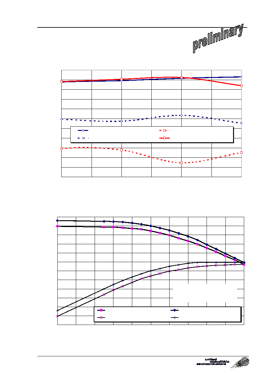
Typical On-wafer Measurements
Bias Conditions : Vdm= Vdl= 3.5 V, Vgm= -0.9V, Vgb= -0.4V, Vgx= -0.8V, Vga= -0.5V
Conversion gain & Image suppression with a 90∞ IQ combiner @ IF=1GHz
Input RF compression by channel
-12
-10
-8
-6
-4
-2
0
2
4
6
8
10
12
-20
-18
-16
-14
-12
-10
-8
-6
-4
-2
0
Input RF power (dBm)
Conversion Gain_I (dB)
Conversion Gain_Q (dB)
IF_power_I (dBm)
IF_power_Q (dBm)
Freq. RF= 38GHz
Freq LO= 18.5GHz
-28
-24
-20
-16
-12
-8
-4
0
4
8
12
16
34
35
36
37
38
39
40
2*LO Frequency (GHz)
Conv
ers
i
on Gain & Image s
uppres
s
i
on (dB)
Gc_channel_inf_rf-
Gc_channel_sup_rf-
Gc_channel_inf_rf+
Gc_channel_sup_rf+

36-40 MFC Down Converter
CHR2296
Ref. : DSCHR22962147 25-May-02
4/5
Specifications subject to change without notice
Route DÈpartementale 128 , B.P.46 - 91401 ORSAY Cedex - FRANCE
Tel.: +33 (0)1 69 33 03 08 - Fax : +33 (0)1 69 33 03 09
Chip Assembly and Mechanical Data
LO
IN
RF
IN
Q
OUT
I
OUT
To Vgm DC Gate Supply
To Vgb DC Gate Supply
To Vgx DC Gate Supply
To Vga DC Gate Supply
To Vdm,Vdl DC Drain Supply
Note : Supply feed should be capacitively bypassed. 25µm diameter gold wire is recommended
Bonding pad positions
( Chip thickness : 100µm. All dimensions are in micrometers )

CHR2296
Ref. : DSCHR22962147 25-May-02
5/5
Specifications subject to change without notice
Route DÈpartementale 128 , B.P.46 - 91401 ORSAY Cedex - FRANCE
Tel.: +33 (0)1 69 33 03 08 - Fax : +33 (0)1 69 33 03 09
Ordering Information
Chip form
:
CHR2296-99F/00
Information furnished is believed to be accurate and reliable. However United Monolithic Semiconductors
S.A.S. assumes no responsibility for the consequences of use of such information nor for any infringement of
patents or other rights of third parties which may result from its use. No license is granted by implication or
otherwise under any patent or patent rights of United Monolithic Semiconductors S.A.S.. Specifications
mentioned in this publication are subject to change without notice. This publication supersedes and replaces all
information previously supplied. United Monolithic Semiconductors S.A.S. products are not authorised for use
as critical components in life support devices or systems without express written approval from United
Monolithic Semiconductors S.A.S.