 | –≠–ª–µ–∫—Ç—Ä–æ–Ω–Ω—ã–π –∫–æ–º–ø–æ–Ω–µ–Ω—Ç: CHU2277 | –°–∫–∞—á–∞—Ç—å:  PDF PDF  ZIP ZIP |
CHU2277
Ref. DSCHU22771074 -15-Mar.-01
1/
7
Specifications subject to change without notice
United Monolithic Semiconductors S.A.S.
Route DÈpartementale 128 - B.P.46 - 91401 Orsay Cedex France
Tel. : +33 (0)1 69 33 03 08 - Fax : +33 (0)1 69 33 03 09
W-band Multifunction : Multiplier / MPA
GaAs Monolithic Microwave IC
Description
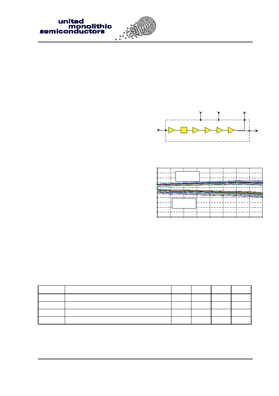
The CHU2277 is a W-band monolithic
multifunction which integrates a frequency
multiplier, a four-stage amplifier and a power
divider. The frequency multiplier is based on an
active transistor and allows to operate at low
input level with a reduced power consumption.
This chip provides two outputs at 77GHz, the
main one is for the transmission path and the
auxiliary one for the receiving mixer (s) LO
signal. All the active devices are internally self
biased. This chip is compatible with automatic
equipment for assembly.
The circuit is manufactured with the P-HEMT
process : 0.15µm gate length, via holes through
the substrate, air bridges and electron beam
gate lithography.
It is available in chip form.
Main Features
n
Wide operating frequency range
n
Low input power : 5dBm typical
n
High output power (OUT1)
n
Auxiliary output power (OUT2)
n
Low AM noise
n
High temperature range
n
On-chip self biasing
n
Automatic assembly oriented
n
Low DC power consumption
n
Chip size : 4.65 x 1.6 x 0.1mm
x2
OUT1
OUT2
IN
+V
-V
W-band multifunction block-diagram
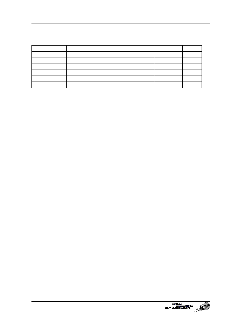
0
2
4
6
8
10
12
14
16
18
20
75
75,5
76
76,5
77
77,5
78
78,5
79
Output frequency (GHz)
O
u
t
put
po
we
r
(
d
Bm)
Typical output power characteristic
Pin = 7dBm
(on wafer measurement)
Main Characteristics
Tamb = +25∞C
Symbol
Parameter
Min
Typ
Max
Unit
F_in
Input frequency
38
38.5
GHz
F_out
Output frequency
76
77
GHz
P_out1
Main output power
13
dBm
P_out2
Auxiliary output power
10
dBm
ESD Protections : Electrostatic discharge sensitive device observe handling precautions !
OUT2
OUT1

CHU2277
W-band Multiplier/MPA
Ref. DSCHU22771074 -15-Mar.-01
2/
7
Specifications subject to change without notice
Route DÈpartementale 128 , B.P.46 - 91401 ORSAY Cedex - FRANCE
Tel.: +33 (0)1 69 33 03 08 - Fax : +33 (0)1 69 33 03 09
Electrical Characteristics
Full operating temperature range, used according to section "Typical assembly and bias
configuration"
Symbol
Parameter
Min
Typ
Max
Unit
F_in
Input frequency
38
38.5
GHz
F_out
Output frequency
76
77
GHz
P_in
Input power
0
5
12
dBm
P_out1
Output power (OUT1) (1)
11
13
16
dBm
P_out2
Output power (OUT2) (1)
8
10
13
dBm
Fin_rej
fundamental rejection (dBc/Pout1(2Fin))
45
55
dBc
S_rej
Spurious rejection (dBc/Pin)
12.75 GHz
25.5 GHz
38.25 GHz
51 GHz
63.75 GHz
76.5 GHz
89.25 GHz
102 GHz
40
40
35
50
40
15
40
50
50
50
45
60
50
20
50
60
dBc
An
Amplitude noise @ 1kHz (SSB)
Amplitude noise @ 10kHz (SSB)
Amplitude noise @ 100kHz (SSB)
Amplitude noise @ 200kHz (SSB)
Amplitude noise @ 1MHz (SSB)
-137
-145
-151
-153
-157
-132
-140
-146
-148
-152
dBc/Hz
VSWR_in
VSWR at input port (50
)
2:1
2.5:1
+V
Positive supply voltage (2)
4.4
4.5
4.6
V
+I
Positive supply current
180
240
mA
-V
Negative supply voltage (2)
-4.6
-4.5
-4.4
V
-I
Negative supply current
14
20
mA
Top
Operating temperature range
-40
100
∞C
(1) Defined on load VSWR
1.5:1.
(2) Negative supply voltage must be applied at least 1us before positive supply
voltage.
W-band Multiplier/MPA
CHU2277
Ref. DSCHU22771074 -15-Mar.-01
3/
7
Specifications subject to change without notice
Route DÈpartementale 128 , B.P.46 - 91401 ORSAY Cedex - FRANCE
Tel.: +33 (0)1 69 33 03 08 - Fax : +33 (0)1 69 33 03 09
Absolute Maximum Ratings (1)
Symbol
Parameter
Values
Unit
P_in
Input power (2)
13
dBm
+V
Positive supply voltage
5
V
-V
Negative supply voltage
-5
V
+I
Positive supply current
250
mA
-I
Negative supply current
20
mA
Tstg
Storage temperature range
-55 to +155
∞C
(1)
Operation of this device above anyone of these parameters may cause permanent damage.
(2)
Duration < 1s

CHU2277
W-band Multiplier/MPA
Ref. DSCHU22771074 -15-Mar.-01
4/
7
Specifications subject to change without notice
Route DÈpartementale 128 , B.P.46 - 91401 ORSAY Cedex - FRANCE
Tel.: +33 (0)1 69 33 03 08 - Fax : +33 (0)1 69 33 03 09
Chip Mechanical Data and Pin References
1
2
3
4
5
6
7
8
9
10
11
12
Unit = µm
External chip size (layout size + dicing streets) = 4650 x 1600
±
35
Chip thickness = 100 +/- 10
HF Pads (2, 5,8) = 68 x 118
DC/IF Pads = 100 x 100
Pin number
Pin name
Description
1,3,4,6,7,9
Ground : should not be bonded. If required,
please ask for more information.
11
Ground (optional)
2
IN
Input port
5
OUT1
Main output
8
OUT2
Auxiliary output
10
+V
Positive supply voltage
12
-V
Negative supply voltage
W-band Multiplier/MPA
CHU2277
Ref. DSCHU22771074 -15-Mar.-01
5/
7
Specifications subject to change without notice
Route DÈpartementale 128 , B.P.46 - 91401 ORSAY Cedex - FRANCE
Tel.: +33 (0)1 69 33 03 08 - Fax : +33 (0)1 69 33 03 09
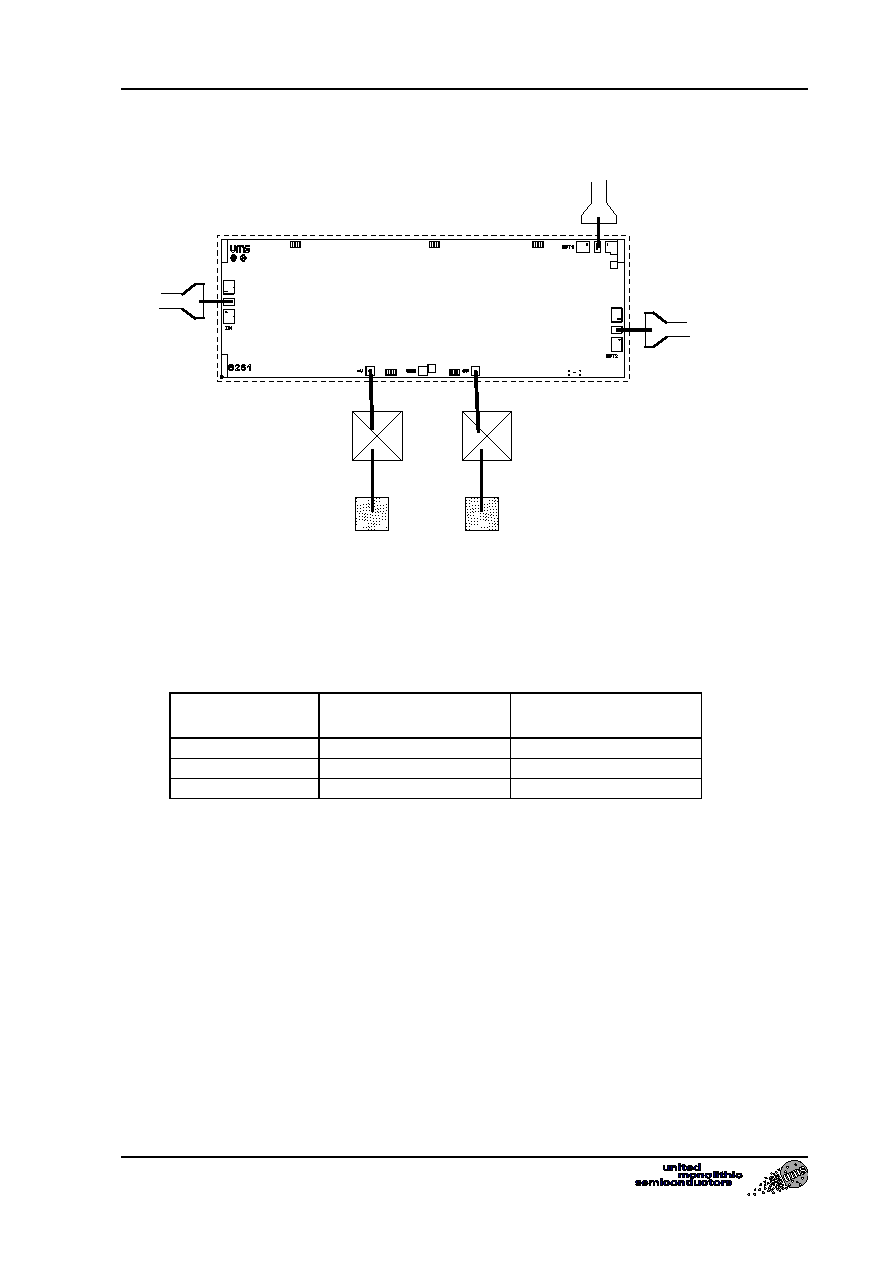
Typical Assembly and Bias Configuration
L_in
-V
+V
µ-strip line
DC lines
>= 120pF
>= 120pF
L_out1
1
2
3
4
5
6
7
8
9
10
11
12
L_out2
µ-strip line
µ-strip line
This drawing shows an example of assembly and bias configuration. All the
transistors are internally self biased. An external capacitor is recommended for
the positive and negative supply voltages.
For the RF pads the equivalent wire bonding inductance (diameter=25µm) have
to be according to the following recommendation.
Port
Equivalent inductance
(nH)
Wire length (mm)
(1)
IN (2)
L_in = 0.32
0.4
OUT1 (5)
L_out1 = 0.32
0.4
OUT2 (8)
L_out2 = 0.32
0.4
(1) This value is the total length including the necessary loop from pad to
pad.
For a micro-strip configuration a hole in the substrate is necessary for chip
assembly.