CHV2241
Ref. : DSCHV22411074 -15-Mar.-01
1/8
Specifications subject to change without notice
united monolithic semiconductors S.A.S.
Route DÈpartementale 128 - B.P.46 - 91401 Orsay Cedex France
Tel. : +33 (0)1 69 33 03 08 - Fax : +33 (0)1 69 33 03 09
K-band Oscillator with integrated Q-band Harmonic
Mixer
GaAs Monolithic Microwave IC
Description
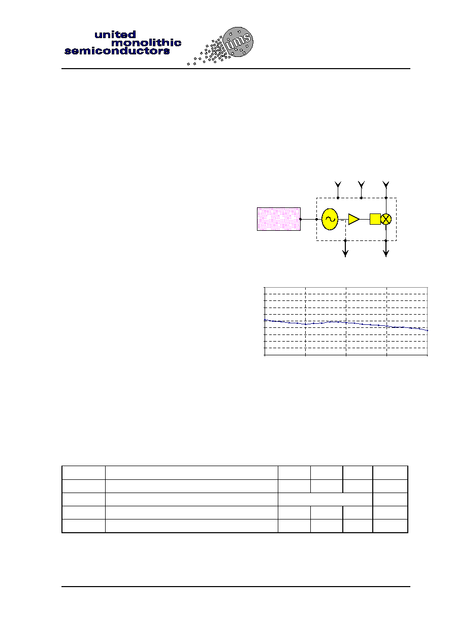
The CHV2241 is a monolithic multifunction
proposed for frequency generation and
transposition. It integrates a K-band oscillator, a
Q-band harmonic mixer and buffer amplifiers.
For performance optimisation, an external port
(ERC) allows a passive resonator coupling to
the oscillator (at half output frequency). All the
active devices are internally self biased.
The circuit is manufactured with the P-HEMT
process : 0.25µm gate length, via holes through
the substrate, air bridges and electron beam
gate lithography.
It is available in chip form.
Main Features
n
K-band Oscillator + Q-band harmonic
mixer
n
External resonator for centre frequency
control and phase noise optimisation
n
High quality oscillator when coupled to
a dielectric resonator
n
Low conversion loss
n
High temperature range
n
On chip self biasing
n
Automatic assembly oriented
n
Chip size 1.82 x 0.97 x 0.1 mm
F_lo = (F_rf - F_if)/2
x2
IF
HIGH Q
RESONATOR
+V
-V
RF
ERC
LO_out_aux
Multifunction block diagram
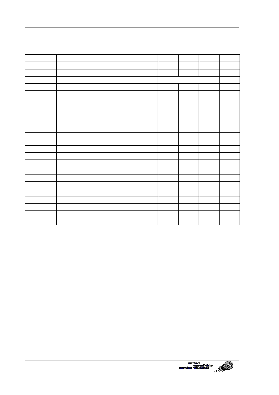
-10
-9
-8
-7
-6
-5
-4
-3
-2
-1
0
37
37,5
38
38,5
39
RF Frequency (GHz)
Co
n
versi
o
n
l
o
ss (d
B)
Typical conversion loss characteristic
Main Characteristics
Tamb = +25∞C
Symbol
Parameter
Min
Typ
Max
Unit
F_rf
RF frequency
37.5
38.25
39
GHz
F_lo
Oscillator frequency
(F_rf - F_if)/2
Pn
Oscillator phase noise @ 100kHz (38GHz)
-100
dBc/Hz
Lc
Conversion loss
7
dB
ESD Protections : Electrostatic discharge sensitive device observe handling precautions !
CHV2241
K-band Oscillator / Q-band Mixer
Ref. : DSCHV22411074 -15-Mar.-01
2/8
Specifications subject to change without notice
Route DÈpartementale 128 , B.P.46 - 91401 ORSAY Cedex - FRANCE
Tel.: +33 (0)1 69 33 03 08 - Fax : +33 (0)1 69 33 03 09
Electrical Characteristics
Full temperature range, used according to section "Typical assembly and bias configuration"
Symbol
Parameter
Min
Typ
Max
Unit
F_rf
RF frequency
37.5
38.25
39
GHz
F_if
IF frequency
0.1
1.5
GHz
F_lo
Oscillator frequency (1)
(F_rf - F_if)/2
P_lo
Auxiliary LO output power (optional)
-15
-8
-4
dBm
Pn
Phase noise (given at RF frequency) (2)
@ 1kHz
@ 10kHz
@ 100kHz
@ 200kHz
@ 1MHz
-45
-78
-105
-114
-129
-35
-68
-95
-104
-119
dBc/Hz
P_V+
Frequency pushing vs positive supply
voltage
300
1000
kHz/v
Lc
Conversion loss
3
7
11
dB
P_1dB_rf
RF input power at 1dB
-13
-8
0
dBm
Plolk_if
LO leakage at IF port (3)
-25
-18
dBm
P2lo_rf
2LO leakage at RF port (3)
-40
-30
dBm
VSWR_rf
VSWR at RF input port
2:1
2.5:1
IMP_if
IF load impedance
50
+V
Positive supply voltage (4)
4.4
4.5
4.6
V
+I
Positive supply current
50
90
mA
-V
Negative supply voltage (4)
-4.6
-4.5
-4.4
V
-I
Negative supply current
6
10
mA
Top
Operating temperature range
-40
+100
∞C
(1) The centre frequency is given by the external passive resonator.
See part "Proposed external high Q resonator" for frequency temperature drift
example.
DRO frequency long term stability is DR environment stability dependant
(hermeticity ...).
(2) This characteristic depends on the external resonator Q, the given performance has
been obtained by using an external dielectric resonator (see section "Proposed External
High Q resonator")
(3) Without external filtering
(4) Negative supply voltage must be applied at least 1us before positive supply
voltage.
K-band Oscillator / Q-band Mixer
CHV2241
Ref. : DSCHV22411074 -15-Mar.-01
3/8
Specifications subject to change without notice
Route DÈpartementale 128 , B.P.46 - 91401 ORSAY Cedex - FRANCE
Tel.: +33 (0)1 69 33 03 08 - Fax : +33 (0)1 69 33 03 09
Absolute Maximum Ratings (1)
Symbol
Parameter
Values
Unit
P_rf
Maximum RF input power (2)
7
dBm
+V
Positive supply voltage
5
V
-V
Negative supply voltage
-5
V
+I
Positive supply current
100
mA
-I
Negative supply current
15
mA
Tstg
Storage temperature range
-55 to +155
∞C
(1)
Operation of this device above anyone of these parameters may cause permanent damage.
(2)
CW mode.

CHV2241
K-band Oscillator / Q-band Mixer
Ref. : DSCHV22411074 -15-Mar.-01
4/8
Specifications subject to change without notice
Route DÈpartementale 128 , B.P.46 - 91401 ORSAY Cedex - FRANCE
Tel.: +33 (0)1 69 33 03 08 - Fax : +33 (0)1 69 33 03 09
Chip Mechanical Data and Pin References
Unit = µm
External chip size (including saw streets)= 1820 x 970 +/- 35
Chip thickness = 100 +/- 10
HF Pads (2, 6) = 68 x 118
DC/IF Pads (+auxiliary LO output) = 100 x 100
Pin number
Pin name
Description
1,3,5,7,8
Ground : should not be bonded. If required,
please ask for more information
2
ERC
External Resonator Coupling Port
4
LO_OUT_AUX Oscillator auxiliary output port (optional)
6
RF
RF input port
9
IF
IF output port
10
NC
11
-V
Negative supply voltage
12,13
+V
Positive supply voltage
1
2
3
4
5
6
7
8
9
10
11
12
13
K-band Oscillator / Q-band Mixer
CHV2241
Ref. : DSCHV22411074 -15-Mar.-01
5/8
Specifications subject to change without notice
Route DÈpartementale 128 , B.P.46 - 91401 ORSAY Cedex - FRANCE
Tel.: +33 (0)1 69 33 03 08 - Fax : +33 (0)1 69 33 03 09
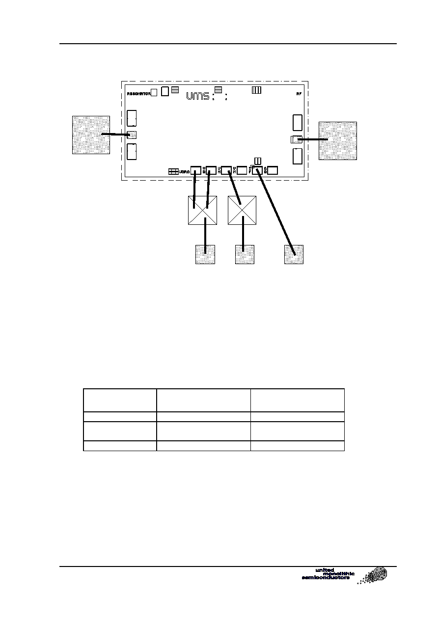
Typical Assembly and Bias Configuration
This drawing shows an example of assembly and bias configuration. All the
transistors are internally self biased. The positive and negative voltages can be
respectively connected together (see drawing) according to the recommended
values given in the electrical characteristics table.
For the RF pads the equivalent wire bonding inductances (diameter=25µm) have
to be according to the following recommendation.
Port
Equivalent inductance
(nH)
Approximative wire
length (mm)
ERC (2)
L_erc = 0.4
0.5
LO_OUT_AUX (4)
Optional
Not critical , < 1nH
RF (6)
L_rf = 0.28
0.35
For a micro-strip configuration a hole in the substrate is recommended for chip
assembly.
1
2
3
4
5
6
7
8
9
10
11
12
13
-V
+V
IF
µ-strip line
µ-strip line
DC and control lines
L_rf
L_erc
>= 120pF
>= 120pF