CHV2244A
Ref. : DSCHV2244A3273 - 01 Oct 03
1/7
Specifications subject to change without notice
United Monolithic Semiconductors S.A.S.
Route DÈpartementale 128 - B.P.46 - 91401 Orsay Cedex France
Tel. : +33 (0)1 69 33 03 08 - Fax : +33 (0)1 69 33 03 09
PRELIMINARY
Fully Integrated HBT Q-band VCO
based on Ku-band Oscillator and Q-band Multiplier
GaAs Monolithic Microwave IC
Description
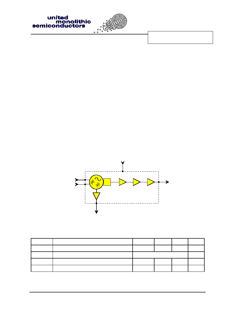
The CHV2244A is a monolithic
multifunction for frequency generation. It
integrates a Ku-band oscillator with
frequency control (VCO), a Q-band filter
and buffer amplifiers. The VCO is fully
integrated on HBT process. On chip base-
collector diodes are used as varactors. Two
tuning ports are available with different
tuning sensitivity. All the active devices are
internally self biased.
The circuit is manufactured on HBT
process: 2µm emitter length, via holes
through the substrate and high Q passive
elements.
Main Features
n Ku-band VCO + Q-band buffers
n Fully integrated VCO
n Two tuning ports
n Low phase noise
n Wide frequency tuning range
n PLL oriented: output at VCO frequency
n High temperature range
n High frequency stability
n On-chip self biasing
n Automatic assembly oriented
n
Chip size 2.0 x 1.46 x 0.1 mm
n
BCB layer protection
RF_out
x3
V_coarse_t
VCO_out_aux
(F_out)
+V
V_fine_t
Multifunction block diagram
Main Characteristics
Tamb = +25∞C
Symbol Parameter Min
Typ
Max
Unit
F_out
Specified output frequency range
38
38.25
38.5
GHz
F_vco Oscillator
frequency
F_out/3
F_tune1 Total output frequency tuning range
5
GHz
Pout Output
power
4
dBm
ESD Protections : Electrostatic discharge sensitive device observe handling precautions !

Q-band VCO
CHV2244A
Ref. : DSCHV2244A3273 - 01 Oct 03
2/7
Specifications subject to change without notice
Route DÈpartementale 128 , B.P.46 - 91401 ORSAY Cedex - FRANCE
Tel.: +33 (0)1 69 33 03 08 - Fax : +33 (0)1 69 33 03 09
PRELIMINARY
Electrical Characteristics
Full temperature range
Symbol Parameter
Min
Typ
Max
Unit
F_out
Specified output frequency range
38
38.25
38.5
GHz
F_vco
VCO frequency
F_out/3
F_tune1
Total frequency tuning range using
V_coarse_tune and V_fine_tune in parallel
(@ F_out)
5 GHz
F_tune2
Frequency tuning range using V_fine_tune
(@ F_out)
1000 MHz
F_tune (T)
Maximum variation of Frequency over
temperature (1)
500
1000
MHz
P_out
Output power on RF_out port (1)
0
4
dBm
H1
Sub-harmonics rejection (Fout/3) (1)
10
dBc
H2
Sub-harmonics rejection (2*Fout/3) (1)
20
dBc
P_VCO
VCO output power on VCO_out_aux port
(1)
-10 -0 dBm
V_coarse_tune
Control voltage range on V_coarse_tune
port
1 - 8
V
V_fine_tune
Control voltage range on V_fine_tune port
1 - 4
V
F_slope_1
Frequency tuning slope using
V_coarse_tune and V_fine_tune in parallel
600 1200
2400 MHz/v
F_slope_2
Frequency tuning slope on V_fine_tune
port
300 600
1200 MHz/v
P_V+
Frequency pushing vs. supply voltage (2)
200
MHz/v
PN
Phase noise (given at F_out) (2)
@ 10kHz
@ 100kHz
@ 1MHz
-52
-82
-109
-47
-77
-104
dBc/
Hz
+V
Positive supply voltage
4.75
5
5.25
V
+I
Positive supply current
180
mA
Top
Operating temperature range
-40
+100
∞C
Specified within F_out (38 to 38.5GHz).
Absolute Maximum Ratings (1)
Symbol Parameter
Values
Unit
V_tune Tuning
voltage
12
V
+V Positive
supply
voltage
6
V
+I
Positive supply current
250
mA
Tstg
Storage temperature range
-55 to +155
∞C
(1)
Operation of this device above anyone of these parameters may cause permanent damage.

Q-band VCO
CHV2244A
Ref. : DSCHV2244A3273 - 01 Oct 03
3/7
Specifications subject to change without notice
Route DÈpartementale 128 , B.P.46 - 91401 ORSAY Cedex - FRANCE
Tel.: +33 (0)1 69 33 03 08 - Fax : +33 (0)1 69 33 03 09
PRELIMINARY
Frequency Characteristics
35
36
37
38
39
40
41
42
1
2
3
4
5
6
7
8
V_coarse_tune (V)
Frequency (
G
H
z
)
Frequency @ 20∞C
Frequency @ 100∞C
Frequency @ -40∞C
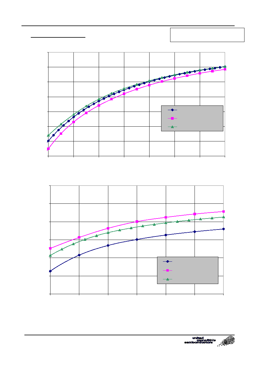
Frequency tuning characteristic (RF_out) with V_coarse_t in parallel with V_fine_t
36
36,5
37
37,5
38
38,5
39
1
1,5
2
2,5
3
3,5
4
V_fine_tune (V)
Frequency (
G
H
z
)
Frequency @100∞C
Frequency @ -40 ∞C
Frequency @ 20∞C
Frequency tuning characteristic on (RF_out) vs. V_coarse_tune
(V_fine_tune = 1 to 4V step 0.25V @ V_coarse_tune=2V)

Q-band VCO
CHV2244A
Ref. : DSCHV2244A3273 - 01 Oct 03
4/7
Specifications subject to change without notice
Route DÈpartementale 128 , B.P.46 - 91401 ORSAY Cedex - FRANCE
Tel.: +33 (0)1 69 33 03 08 - Fax : +33 (0)1 69 33 03 09
PRELIMINARY
Output Powers on Main and Prescalar Ports
-5
-4
-3
-2
-1
0
1
2
3
4
5
1
2
3
4
5
6
7
8
Vtune (V)
Pow
e
r
(
d
B
m
)
Power @ 20∞C
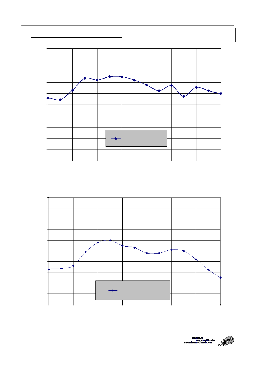
Output Power @ 12.75GHz (VCO_out_aux) vs. V_coarse_tune in parallel with
V_fine_tune
0
1
2
3
4
5
6
7
8
9
10
1
2
3
4
5
6
7
8
Vtune (V)
Po
w
e
r (
d
B
m
)
Power @ 20∞C
Output Power @ 38.25GHz (RF_out) vs. V_coarse_tune in parallel with V_fine_tune

Q-band VCO
CHV2244A
Ref. : DSCHV2244A3273 - 01 Oct 03
5/7
Specifications subject to change without notice
Route DÈpartementale 128 , B.P.46 - 91401 ORSAY Cedex - FRANCE
Tel.: +33 (0)1 69 33 03 08 - Fax : +33 (0)1 69 33 03 09
PRELIMINARY
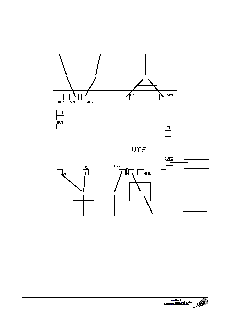
Chip Assembly and Bias Configuration
This drawing shows an example of assembly and bias configuration. All the transistors are
internally self biased. The positive and tuning voltages can be respectively connected together
according to the recommended values given in the electrical characteristics table. Due to the high
value of frequency sensitivity versus tuning voltage (around 1000 MHz/V), the signal applied
to V_coarse_tune and V_fine_tune ports must exhibit very low level of noise.
Out@12.75GHz
100pF
100pF
100pF
100pF
100pF
100pF
To V_coarse_tune DC supply feed
To V_fine_tune DC supply feed
To +V DC Collector supply feed
To +V DC Collector supply feed
To V_coarse_tune DC supply feed
To V_fine_tune DC supply feed
Out@38.25GHz
