
US1206/1207/1208/1209
2-1
Rev. 1.1
6/26/00
TYPICAL APPLICATION
TYPICAL APPLICATION
DESCRIPTION
DESCRIPTION
The US1206 family of devices are ultra low dropout 1A
regulators using PNP transistor as the pass element.
These products are ideal when a single input supply is
available only and the dropout voltage is less than 1V,
exceeding the minimum dropout characteristics of NPN/
PNP hybrid regulators. One common application of these
regulators are where input is 3.3V and a 2.5V output is
needed.
Besides the low dropout of less than 0.5V, other fea-
tures of the family of the parts are; micropower shutdown
capability and output UVLO detection where Flag pin is
switched low when output is below 5% of its nominal
point. The US1206-XX in SOT223 is pin compatible with
MIC39100-XX, US1207 and 1209 in SO8 power package
are compatible with MIC39101 and 39102 respectively.
1A ULTRA LOW DROPOUT POSITIVE
ADJUSTABLE & FIXED REGULATOR
FEATURES
FEATURES
Low Droput Voltage (500mV at 1A)
1% Voltage Reference Accuracy
Low Ground Current
10uA Quiescent Current in Shutdown
(US1207,1208)
Fast Transient Response
Current Limit and Thermal Shutdown
Error Flag Signal for Output out of Regulation
(US1207,1209)
Pin Compatible with MIC39100/101/102 series
APPLICATIONS
APPLICATIONS
2.5V Supply from 3.3V Input for the new genera-
tion of Logic ICs
Computer Mother Board, Add on Cards
High Efficiency Post Regulator in SMPS
PRELIMINARY DATASHEET
PACKAGE ORDER INFORMATION
PACKAGE ORDER INFORMATION
Vin
Vout
C1
C2
1206app1-1.0
US1206-XX
1
2
3
Vin
Gnd
Vout
Tj (�C) 3 LEAD 5 LEAD 8 PIN PLASTIC Voltage Pin Functions
TO252 TO263 SOIC Power
0 TO 125 US1206-18CD US1206-18CY US1206-18CM 1.8V Vin, Vout, GND
0 TO 125 US1206-25CD US1206-25CY US1206-25CM 2.5V Vin, Vout, GND
0 TO 125 US1206-33CD US1206-33CY US1206-33CM 3.3V Vin, Vout, GND
0 TO 125 NA US1207-18CM US1207CS 1.8V Vin, Vout, GND, Enable, Flag
0 TO 125 NA US1207-25CM US1207CS 2.5V Vin, Vout, GND, Enable, Flag
0 TO 125 NA US1207-33CM US1207CS 3.3V Vin, Vout, GND, Enable, Flag
0 TO 125 NA US1208CM US1208CS Adj Vin, Vout, GND, Flag, Adj
0 TO 125 NA US1209CM US1209CS Adj Vin, Vout, GND, Adj, Enable
2-2
Rev. 1.1
6/26/00
US1206/1207/1208/1209
Unless otherwise specified ,these specifications apply over ,Cin=Cout=10uF,Vin=Vo+1V, Vout=Vfb (for adjustable
version only), and Ta=25
�
C. Typical values refer to Ta=25
�
C.Low duty cycle pulse testing are used which keeps
junction and case temperatures equal to the ambient temperature.
PARAMETER
SYM
TEST CONDITION
MIN
TYP MAX
UNITS
Reference Voltage
Vo
Io=10mA
-1
1
%
See Table 1 for typical values
(Note 4)
-2
2
Line Regulation
dVi
Vo+1V<Vin<12
0.06
%/V
Load Regulation (note 1)
dVL
10mA<Io<1A
0.7
%
1mA<Io<150mA
0.5
%
Output voltage Temp Coef.
dVoT
20
100 ppm/
�
C
Dropout Voltage (note 2)
dVio
Io=100mA (Note 4)
100
200
mV
Io=500mA (Note 4)
300
400
mV
Io=1000mA (Note 4)
500
650
mV
Ground Current (Note 3)
Iq
Vin=Vo +1
Io=100mA (Note 4)
3
mA
Io=500mA (Note 4)
15
mA
Io=1000mA (Note 4)
50
mA
Current Limit
Icl
Vo=0V
1.1
A
Minimum Input Voltage Vinmin
2.1
2.3
V
US1208,1209
Adjust Pin Current
Iadj
Vin=2.5V,Vo=Vadj (Note 4)
0.1
uA
Minimum Load Current Iomin
1
mA
ABSOLUTE MAXIMUM RATINGS
ABSOLUTE MAXIMUM RATINGS
Input Voltage (Vin) ............................................................. 12V
Enable Input Voltage ........................................................... 12V
Storage Temperature Range ................................ -65�C TO 150�C
Operating Junction Temperature Range ...................... 0�C TO 135�C
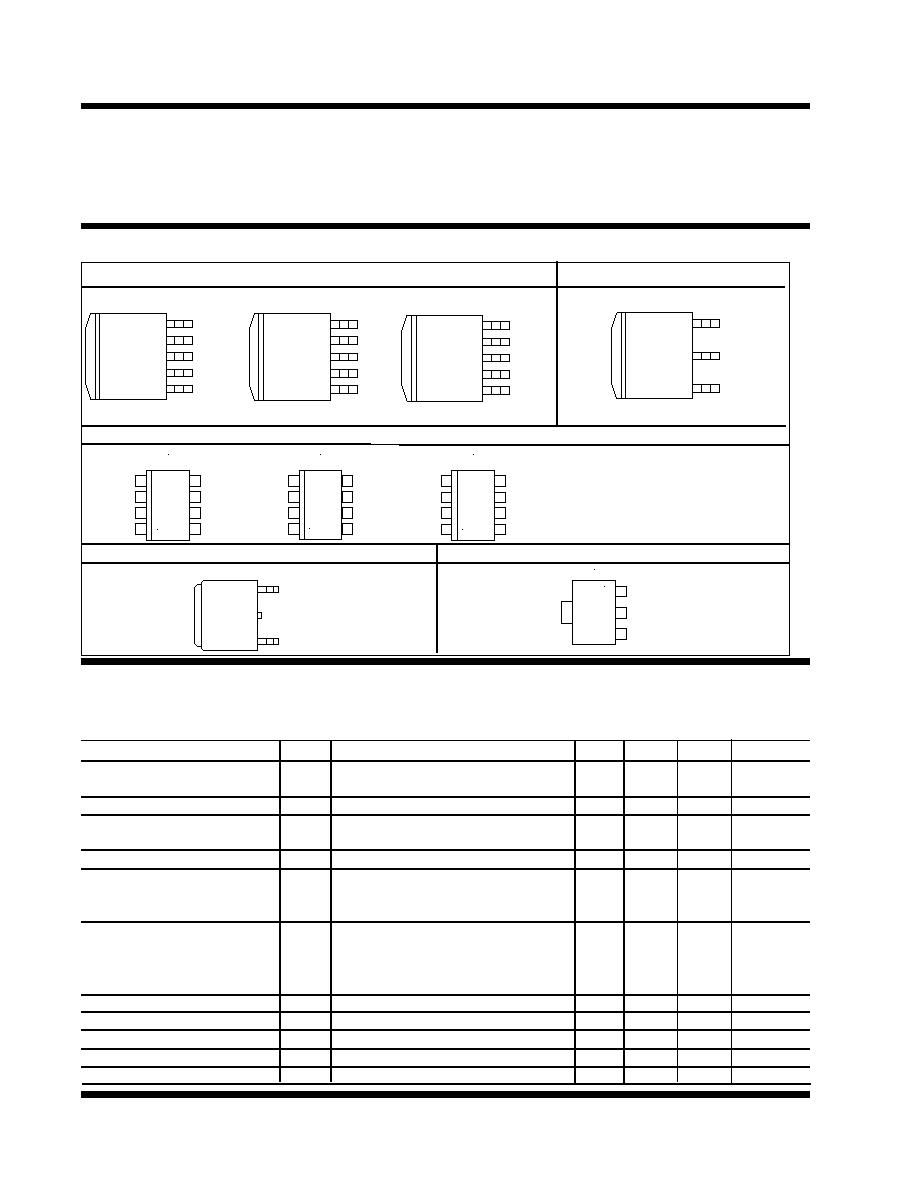
PACKAGE INFORMATION
PACKAGE INFORMATION
ELECTRICAL SPECIFICATIONS
ELECTRICAL SPECIFICATIONS
5 PIN PLASTIC TO263 ( M ) or 5 PIN POWER FLEX (P)
3 PIN PLASTIC TO263 ( M )
US1207 US1208 US1209
US1206-XX
JA
=35
�
C/W for 0.5" square pad
JA
=35
�
C/W for 0.5" square pad
FRONT VIEW
1
2
3
Vin
Gnd
Vout
FRONT VIEW
1
2
3
4
5
Enable
Vin
Gnd
Vout
Flag
8 PIN PLASTIC POWER SOIC ( S )
US1207 US1208 US1209
4
3
2
1
5
6
7
8
TOP VIEW
Gnd
Flag
Vout
Vin
Enable
Gnd
Gnd
Gnd
JA
=55
�
C/W for 1" Sq pad
3 PIN PLASTIC TO252 ( D )
3 PIN PLASTIC SOT223 ( Y )
US1206
US1206
1
4
3
FRONT VIEW
Vin
Vout
Tab is
Gnd
JA
=70
�
C/W for
0.5" Sq pad
JA
=90
�
C/W for
0.4" Sq pad
3
1
2
TOP VIEW
Vin
Gnd
Vout
Tab is
Gnd
FRONT VIEW
1
2
3
4
5
Flag
Vin
Gnd
Vout
Adj
FRONT VIEW
1
2
3
4
5
Enable
Vin
Gnd
Vout
Adj
4
3
2
1
5
6
7
8
TOP VIEW
Gnd
Adj
Vout
Vin
Flag
Gnd
Gnd
Gnd
4
3
2
1
5
6
7
8
TOP VIEW
Gnd
Adj
Vout
Vin
Enable
Gnd
Gnd
Gnd

US1206/1207/1208/1209
2-3
Rev. 1.1
6/26/00
Pin DescRIPTIONS
Pin DescRIPTIONS
PIN DESCRIPTION
A resistor divider from this pin to the Vout pin and ground sets
the output voltage.
An open collector output that switches low when the output
voltage drops about 4% below its expected regulated voltage.
The output of the regulator .A minimum of 2.2uF capacitor
must be connected from this pin to ground.
Ground pin. This pin must be connected to the lowest poten-
tial in the system & all other pins must be at higher potential
with respect to this pin.
Enable pin. A low signal or left open on this pin shuts down the
output.This pin must be tied HI or to Vin for normal operation.
The input pin of the regulator. Typically a large storage
capacitor is connected from this pin to ground to insure that
the input voltage does not sag below the minimumdrop out
voltage during the load transient response. This pin must al-
ways be 0.6V higher than Vout in order for thedevice to regu-
late properly.
APPLICATION INFORMATION
APPLICATION INFORMATION
Stability
The US120X series of regulators require the use of an
output capacitor as part of the frequency compensation
in order to make the regulator stable. A minimum of
2.2uF capacitance and the ESR in the range of 0.5 to 2
ohm insures the stability of the system.
Part Number Output
Voltage
US1206-18 1.8V
US1206-25 2.5V
US1206-33 3.3V
US1207-18 1.8V
US1207-25 2.5V
US1207-33 3.3V
US1208 1.24V
US1209 1.24V
Table 1- Output voltage v.s. part number
Note 1 : Low duty cycle pulse testing with Kelvin con-
nections are required in order to maintain accurate data.
Note 2 : Drop-out voltage is defined as the minimum
differential voltage between Vin and Vout required to main-
tain regulation at Vout. It is measured when the output
voltage drops 1% below its nominal value.
US1207,1208
SYM
TEST CONDITION
MIN
TYP MAX
UNITS
Ground Current-S.D Activated
Iqsd
Enable=0V
0.01
1
uA
Enable pin input LO voltage
Venl
Regulator OFF (Note 4)
0.8
V
Enable pin input HI voltage
Venh
Regulator ON (Note 4)
2
V
Enable pin input LO current
Venl=0V to 0.8V (Note 4)
0.1
2
uA
Enable pin input HI current
Venh=2V to Vin (Note 4)
100
600
uA
US1207,1209
Flag Output Threshold Voltage Vthfg
3.8
%Vo
Flag Output Hysterises Voltage Vhys
Output Ramping Up
0.8
%Vo
Flag Output Saturation Voltage Vfsat
Io=5mA
400
mV
Io=500uA
230
mV
Note 3 : Ground current is the the regulator quiescent
current plus the pass transistor current. The total cur-
rent from the supply is the sum of the load current plus
the ground pin current.
Note 4 : The specification applies for the junction tem-
perature of 0 to +125
�
C.
PIN SYMBOL
Adj
US1208,1209
Flag
US1208
Vout
All devices
GND
All devices
Enable
US1207,1209
Vin
All devices

2-4
Rev. 1.1
6/26/00
US1206/1207/1208/1209
TYPICAL APPLICATION
TYPICAL APPLICATION
Ref Desig
Description
Qty
Part #
Manuf
C1
Capacitor
1
10uF, Tantalum
AVX
C2
Capacitor
1
10uF, Tantalum
AVX
Figure 1- Typical application of US1206
Vin
Vout
C1
C2
1206app1-1.0
US1206-XX
1
2
3
Vin
Gnd
Vout

US1206/1207/1208/1209
2-5
Rev. 1.1
6/26/00
Vin
Vout
R1
C1
C2
1207app1-1.0
S.D.
Enable
1
2
3
4
5
Enable
Vin
Gnd
Vout
Flag
US1207
Error Flag
TYPICAL APPLICATION
TYPICAL APPLICATION
Ref Desig
Description
Qty
Part #
Manuf
C1
Capacitor
1
10uF, Tantalum
AVX
C2
Capacitor
1
10uF, Tantalum
AVX
R1
Resistor
1
10k
, 5%
Panasonic
Figure 1- Typical application of US1207
Pin numbers in this
schematic apply only
to TO263(M) package.