 | –≠–ª–µ–∫—Ç—Ä–æ–Ω–Ω—ã–π –∫–æ–º–ø–æ–Ω–µ–Ω—Ç: US1261CM | –°–∫–∞—á–∞—Ç—å:  PDF PDF  ZIP ZIP |
US1261
3-1
Rev. 1.7
3/22/99
PACKAGE ORDER INFORMATION
PACKAGE ORDER INFORMATION
TYPICAL APPLICATION
TYPICAL APPLICATION
FEATURES
FEATURES
Guaranteed to provide 1.5V and 2.5V Sup-
plies with 3.1V input.
Fast Transient Response
1% Voltage Reference Initial Accuracy
Built in Thermal Shutdown
APPLICATIONS
APPLICATIONS
Pentium II Processor Applications
DESCRIPTION
DESCRIPTION
The US1261 product using a proprietary process com-
bines a dual low dropout regulators with fixed outputs of
1.5V and 2.5V in a single package with the 1.5V out-
put having a minimum of 6A and the 2.5V having a 1A
output current capability. This product is specifically de-
signed to provide well regulated supplies from 3.3V to
generate 1.5V for GTL+ termination resistor supply
and 2.5V clock supply for the new generation of
the Pentium II processor applications.
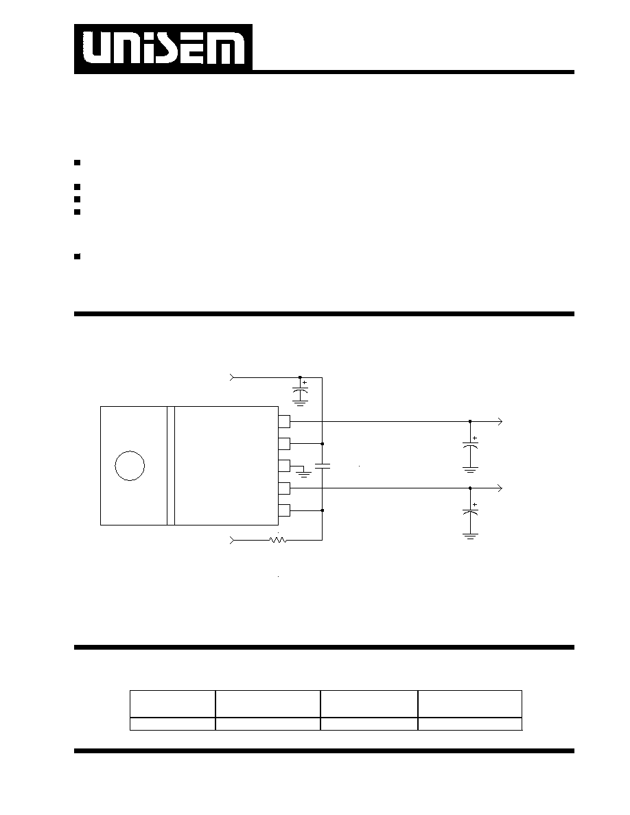
DUAL 6A AND 1A LOW DROPOUT
POSITIVE FIXED OUTPUT REGULATOR
Typical application of US1261 in a Pentium II processor application
3.3V
2.5V / 1A
US1261
1.5V / 6A
C1
C3
C4
1261app1-1.3
5V
C2
1
2
3
4
5
Vctrl
Vout2
Gnd
Vin
Vout1
R1
Tj (
∞
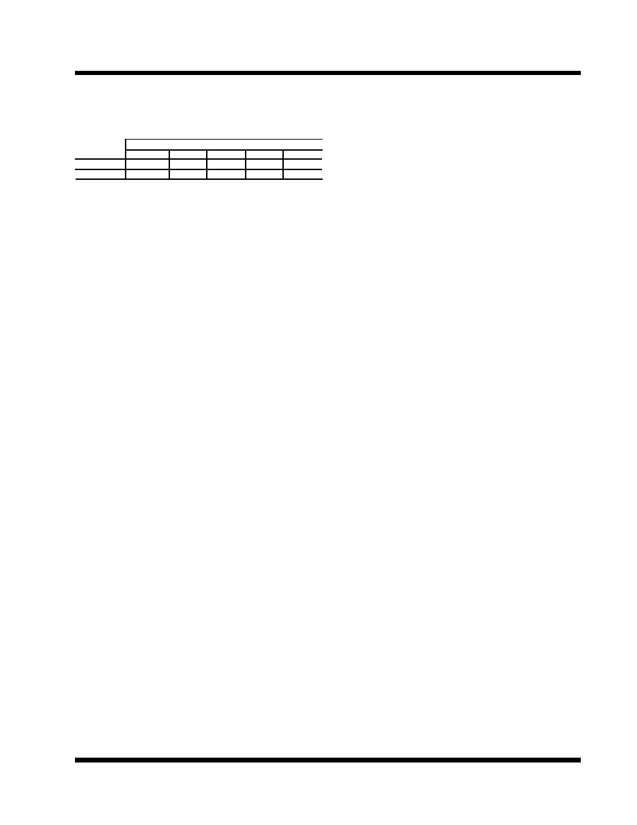
C) 5 PIN PLASTIC 5 PIN PLASTIC 5 PIN PLASTIC
TO220(T) TO263(M) POWER FLEX(P)
0 TO 150 US1261CT US1261CM US1261CP
US1261
3-2
Rev. 1.7
3/22/99
Unless otherwise specified ,these specifications apply over ,Cin=1 uF,Cout=100uF,and Tj=0 to 150
∞
C.Typical
values refer to Tj=25
∞
C. Ifl=6A for output #2 & 1A for output #1.Vctrl=5V,Vin=3.3V.
PARAMETER
SYM
TEST CONDITION
MIN
TYP
MAX
UNITS
Vctrl Input Voltage
3.0
V
Output Voltage #2 Vo2
Io=10mA, Tj=25
∞
C 1.485 1.500
1.515 V
Io=10mA 1.470 1.500
1.530
Output Voltage #1 Vo1
Io=10mA, Tj=25
∞
C 2.462 2.500
2.537 V
Io=10mA 2.425 2.500
2.575
Line Regulation
Io=10mA, 3.1V<Vin<3.6V
0.2
%
Load Regulation (note 1)
10mA<Io<Ifl
0.4
%
Dropout Voltage (output #2)
Note 2,
Io=6A, Vctrl=4.75V
1.3
V
Dropout Voltage (output #1)
Note 2,
Io=1A, Vctrl=4.75V
0.4
0.6
V
Current Limit (output #2)
dVo=100mV
6.1
A
Current Limit (output #1)
dVo=100mV
1.1
A
Minimum Load Current
5
10
mA
(note 3)
Thermal Regulation
30 mS PULSE,Io=Ifl
0.01
0.02
%/W
Ripple Rejection
f=120HZ ,Co=25uF Tan
Io=0.5*Ifl
70 dB
Temperature Stability
Io=10mA
0.5
%
Long Term Stability
Tj=125
∞
C,1000 Hrs
0.3
%
RMS Output Noise
10hz<f<10khz
0.003
%Vo
Note 3 : Minimum load current is defined as the mini-
mum current required at the output in order for the out-
put voltage to maintain regulation. Typically the resistor
dividers are selected such that it automatically main-
tains this current.
ABSOLUTE MAXIMUM RATINGS
ABSOLUTE MAXIMUM RATINGS
Input Voltage (Vin) ............................................................. 10V
Power Dissipation ............................................ Internally Limited
Storage Temperature Range ................................ -65
∞
C TO 150
∞
C
Operating Junction Temperature Range ...................... 0
∞
C TO 150
∞
C
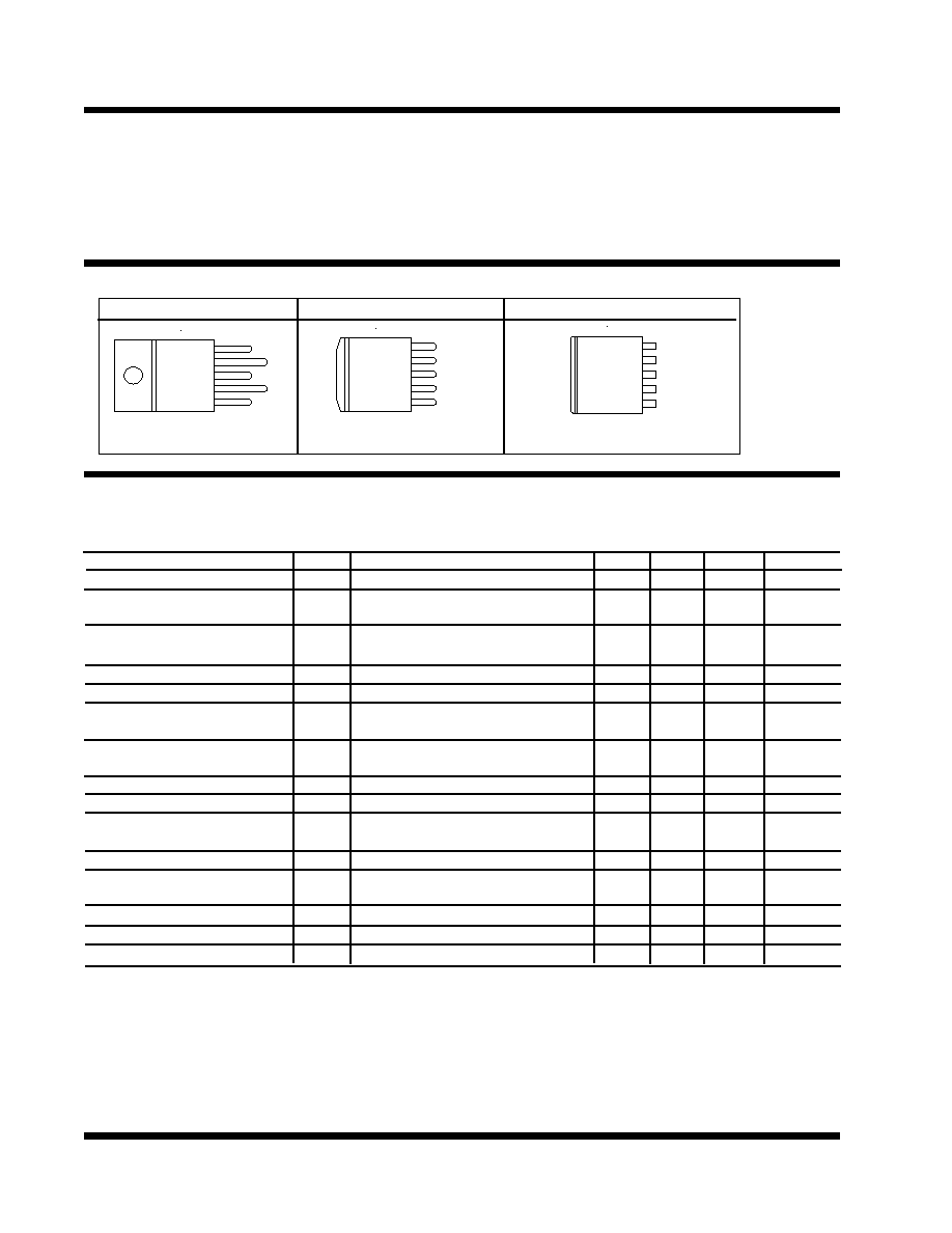
PACKAGE INFORMATION
PACKAGE INFORMATION
7 PIN PLASTIC TO220
7 PIN PLASTIC TO263
7 PIN POWER FLEX (P)
JT
=2.7
∞
C/W
JA
=60
∞
C/W
JA
=30
∞
C/W for 1"sq pad
JA
=30
∞
C/W for 1"sq pad
ELECTRICAL SPECIFICATIONS
ELECTRICAL SPECIFICATIONS
Note 1 : Low duty cycle pulse testing with Kelvin con-
nections are required in order to maintain accurate data.
Note 2 : Drop-out voltage is defined as the minimum
differential voltage between Vin and Vout required to main-
tain regulation at Vout. It is measured when the output
voltage drops 1% below its nominal value.
FRONT VIEW
1
2
3
4
5
Vctrl
Gnd
Vout2
Vin
Vout1
Vctrl
Gnd
Vout2
Vin
Vout1
FRONT VIEW
1
2
3
4
5
FRONT VIEW
1
2
3
4
5
Vctrl
Gnd
Vout2
Vin
Vout1
US1261
3-3
Rev. 1.7
3/22/99
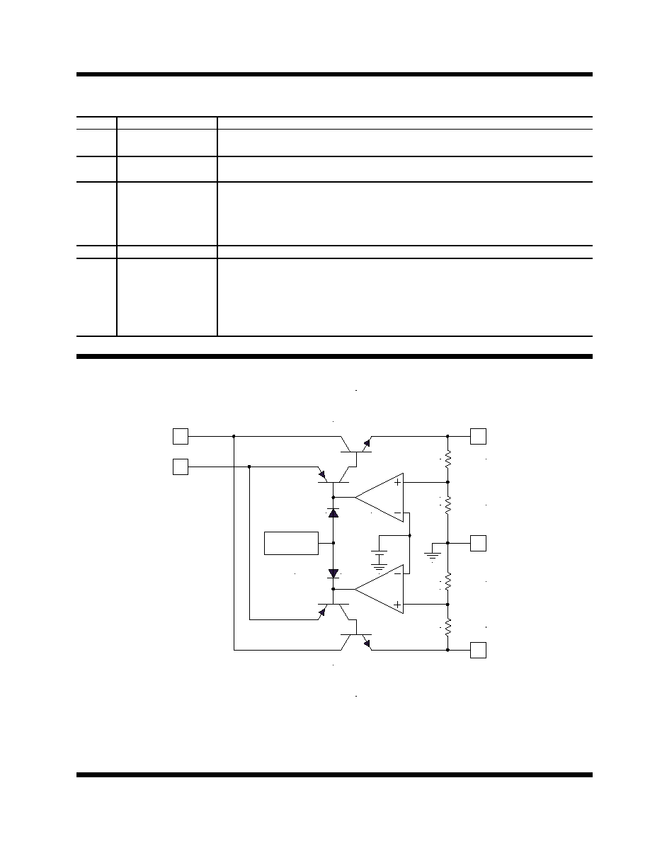
BLOCK DIAGRAM
BLOCK DIAGRAM
PIN DESCRIPTIONS
PIN DESCRIPTIONS
PIN #
PIN SYMBOL PIN DESCRIPTION
2
Vout2
The output #2 (high current) of the regulator. A minimum of 100uF capacitor
must be connected from this pin to ground to insure stability.
5
Vout1
The output #1 (low current) of the regulator. A minimum of 100uF capacitor
must be connected from this pin to ground to insure stability.
4
Vin
The power input pin of the regulator. Typically a large storage capacitor is
connected from this pin to ground to insure that the input voltage does not sag
below the minimum drop out voltage during the load transient response. This
pin must always be higher than both Vout pins by the amount of the dropout
voltage(see datasheet) in order for the device to regulate properly.
3
Gnd
This pin is connected to GND. It is also the TAB of the package.
1
Vctrl
The control input pin of the regulator. This pin via a 10
resistor is connected
to the 5V supply to provide the base current for the pass transistor of both
regulators. This allows the regulator to have very low dropout voltage
which allows one to generate a well regulated 2.5V supply from the 3.3V input.
A high frequency, 1 uF capacitor is connected between this pin and Vin pin to
insure stability.
Figure 1 - Simplified block diagram of the US1261
Vctrl
Vin
Gnd
4
1
3
1261blk1-1.1
2 Vout2
5 Vout1
THERMAL
SHUTDOWN
1.20V
+
US1261
3-4
Rev. 1.7
3/22/99
APPLICATION INFORMATION
APPLICATION INFORMATION
Introduction
The US1261 is a dual fixed output Low Dropout (LDO)
regulator available in a 5 pin TO-220 or TO-263 pack-
ages. This voltage regulator is designed specifically for
PentiumII processor applications requiring 2.5V and 1.5
V supplies, eliminating the need for a second regu-
lator resulting in lower overall system cost. The
US1261 is designed to take advantage of 5V supply to
provide the drive for the pass transistor, allowing 2.5V
supply to be generated from 3.3V input.This feature im-
proves the power dissipation of the 2.5V regulator sub-
stantially allowing a smaller heat sink to be used for the
application. Compared to the US1260 dual adjustable
regulator, the US1261 includes the resistor dividers that
are otherwise needed with the US1260, eliminating 4
external components and their tolerances, resulting in a
more accurate initial accuracy for each output voltage.
Other features of the device include; fast response to
sudden load current changes, such as GTL+ termina-
tion application and thermal shutdown protection to pro-
tect the device if an overload condition occurs.
Stability
The US1261 requires the use of an output capacitor as
part of the frequency compensation in order to make the
regulator stable. Typical designs for the microproces-
sor applications use standard electrolytic capacitors with
typical ESR in the range of 50 to 100 m
and the output
capacitance of 500 to 1000uF. Fortunately as the ca-
pacitance increases, the ESR decreases resulting in a
fixed RC time constant. The US1261 takes advantage of
this phenomena in making the overall regulator loop
stable. For most applications a minimum of 100uF alu-
minum electrolytic capacitor with the maximum ESR of
0.3
such as Sanyo, MVGX series ,Panasonic FA se-
ries as well as the Nichicon PL series insures both sta-
bility and good transient response. The US1261 also
requires a 1 uF ceramic capacitor connected from Vin
to Vctrl and a 10
, 0.1
W resistor in series with Vctrl pin
in order to further insure stability.
Thermal Design
The US1261 incorporates an internal thermal shutdown
that protects the device when the junction temperature
exceeds the maximum allowable junction temperature.
Although this device can operate with junction tempera-
tures in the range of 150
∞
C ,it is recommended that the
selected heat sink be chosen such that during maxi-
mum continuous load operation the junction tempera-
ture is kept below this number. Two examples are given
which shows the steps in selecting the proper regulator
heat sink for driving the Pentium II processor GTL+ ter-
mination resistors and the Clock IC using 1261 in TO220
and TO-263 packages.
Example # 1
Assuming the following specifications :
The steps for selecting a proper heat sink to keep the
junction temperature below 135
∞
C is given as :
1) Calculate the maximum power dissipation using :
2) Select a package from the datasheet and record its
junction to case (or Tab) thermal resistance.
Selecting TO220 package gives us :
3) Assuming that the heat sink is Black Anodized, cal-
culate the maximum Heat sink temperature allowed :
Assume ,
CS
= 0.05
∞
C/W (Heat sink to Case thermal
resistance for Black Anodized)
4) With the maximum heat sink temperature calculated
in the previous step, the Heat Sink to Air thermal resis-
tance
SA
is calculated as follows :
5) Next , a heat sink with lower
SA
than the one calcu-
lated in step 4 must be selected. One way to do this is
to simply look at the graphs of the "Heat Sink Temp
Rise Above the Ambient" vs. the "Power Dissipation" and
V
3.3V
V
1.5 V
V
= 2.5 V
I
5.4A
I
= 0.4 A
T
35 C
IN
OUT 2
OUT 1
OUT 2
OUT 1
A
MAX
MAX
=
=
=
=
∞
(
)
(
)
T
T
P
T
135
10
2.7
0.05
107.4 C
S
J
D
S
=
-
◊
+
=
-
◊
+
=
∞
JC
CS
T
S
A
T
T
C
=
-
=
-
=
∞
107 4
35
72 4
.
.
SA
T
D
SA
P
C W
=
=
=
∞
72 4
10
7 24
.
.
/
(
)
(
)
(
)
(
)
P
I
V
V
I
V
V
P
0.4
+ 5.4
3.3
1.5
W
D
OUT1
IN
OUT1
OUT2
IN
OUT2
D
=
◊
-
+
◊
-
=
◊
-
◊
-
=
3 3
2 5
10
.
.
JC
C W
=
∞
2 7
.
/
US1261
3-5
Rev. 1.7
3/22/99
Example # 2
:
Assuming the following specifications :
The steps for selecting a proper heat sink to keep the
junction temperature below 135
∞
C is given as :
1) Calculate the maximum power dissipation using :
2) Assuming a TO-263 surface mount package, the junc-
tion to ambient thermal resistance of the package is:
Air Flow (LFM)
0 100 200 300 400
Thermalloy 7021B 7020B 6021PB 7173D 7141D
AAVID 593101B 551002B 534202B 577102B 576802B
Note : For further information regarding the above com-
panies and their latest product offering and application
support contact your local representative or the num-
bers listed below:
Thermalloy
PH# (214) 243-4321
AAVID
PH# (603) 528-3400
3) The maximum junction temperature of the device is cal-
culated using the equation below :
Since this is lower than our selected 135
∞
C maximum junc-
tion temperature (150
∞
C is the thermal shutdown of the
device), TO-263 package is a suitable package for our ap-
plication.
select a heat sink that results in lower temperature rise
than the one calculated in previous step. The following
heat sinks from AAVID and Thermaloy meet this crite-
ria.
Layout Consideration
The US1261 like all other high speed linear regulators need
to be properly laid out to insure stable operation. The most
important component is the output capacitor, which
needs to be placed close to the output pin and con-
nected to this pin using a plane connection with a
low inductance path.
V
3.3V
V
1.5 V
V
= 2.5 V
I
1.5A
I
= 0.2 A
T
35 C
IN
OUT 2
OUT 1
OUT 2
OUT 1
A
MAX
MAX
=
=
=
=
∞
(
)
(
)
(
)
(
)
P
I
V
V
I
V
V
P
0.2
3.3
2.5 + 1.5
3.3
1.5
2.86 W
D
OUT1
IN
OUT1
OUT2
IN
OUT2
D
=
◊
-
+
◊
-
=
◊
-
◊
-
=
JA
C W for 1"
=
∞
30
/
square pad area
T
T
P
T
35 + 2.86
30 = 121 C
J
A
D
J
=
+
◊
=
◊
∞
JA