US3018
4-1
Rev. 1.4
12/8/00
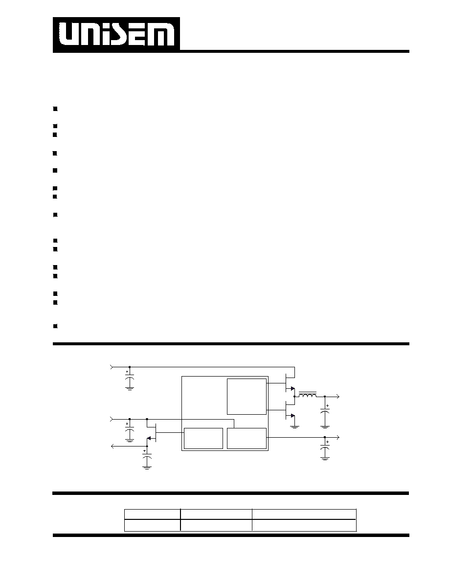
TYPICAL APPLICATION
TYPICAL APPLICATION
DESCRIPTION
DESCRIPTION
The US3018 controller IC is specifically designed to meet
Intel specification for Pentium II
TM
microprocessor ap-
plications as well as the next generation of P6 family
processors. The US3018 provides a single chip con-
troller IC for the Vcore , LDO controller for GTL+
and an internal 200mA regulator for clock supply
which are required for the Pentium II applications.
These devices feature a patented topology that in com-
bination with a few external components as shown in
the typical application circuit ,will provide in excess of
18A of output current for an on- board DC/DC converter
while automatically providing the right output voltage via
the 5 bit internal DAC. The US3018 also features, loss
less current sensing for both switchers by using the
Rds-on of the high side Power MOSFET as the sens-
ing resistor, internal current limiting for the clock
supply, a Power Good window comparator that switches
its open collector output low when any one of the out-
puts is outside of a pre programmed window. Other fea-
tures of the device are ; Undervoltage lockout for both
5V and 12V supplies, an external programmable soft
start function , programming the oscillator frequency via
an external resistor, OVP circuitry for both switcher out-
puts and an internal thermal shutdown.
Provides Single Chip Solution for Vcore, GTL+
& Clock Supply
200 mA On board LDO regulator
Designed to meet the latest Intel specification
for Pentium II
TM
On board DAC programs the output voltage
from 1.3V to 3.5V
Linear regulator controller on board for 1.5V
GTL+ supply
Loss less Short Circuit Protection with HICCUP
Synchronous operation allows maximum effi-
ciency
Patented architecture allows fixed frequency
operation as well as 100% duty cycle during
dynamic load
Soft Start
High current totem pole driver for direct driv-
ing of the external Power MOSFET
Power Good function Monitors all Outputs
OVP Circuitry Protects the Switcher Output and
generates a Fault signal
Thermal Shutdown
Logic Level Enable Input
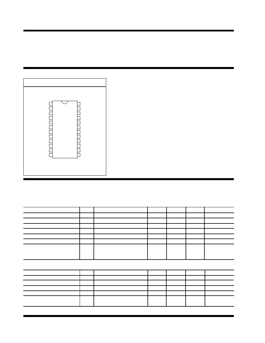
PACKAGE ORDER INFORMATION
PACKAGE ORDER INFORMATION
PRELIMINARY DATASHEET
FEATURES
FEATURES
5 BIT PROGRAMMABLE SYNCHRONOUS BUCK PLUS
LDO CONTROLLER AND 200mA LDO ON BOARD
APPLICATIONS
APPLICATIONS
Total Power Soloution for Pentium II processor
application
Notes: Pentium II is trade mark of Intel Corp.
Ta (
�
C) Device Package
0 TO 70 US3018CW 24 pin Plastic SOIC WB
3018app3-1.1
LINEAR
CONTROL
LINEAR
REGULATOR
SWITCHER1
CONTROL
US3018
Vout3
5V
Vout1
Vout2
3.3V
4-2
Rev. 1.4
12/8/00
US3018
ELECTRICAL SPECIFICATIONS
ELECTRICAL SPECIFICATIONS
Unless otherwise specified ,these specifications apply over ,V
12
= 12V, V
5
= 5V and Ta=0 to 70
�
C. Typical values
refer to Ta =25
�
C. Low duty cycle pulse testing are used which keeps junction and case temperatures equal to the
ambient temperature.
PARAMETER
SYM
TEST CONDITION
MIN
TYP
MAX
UNITS
Supply UVLO Section
UVLO Threshold-12V
Supply ramping up
10
V
UVLO Hysterises-12V
0.4
V
UVLO Threshold-5V
Supply ramping up
4.3
V
UVLO Hysterises-5V
0.3
V
Supply Current
Operating Supply Current
I
12
V12
6
mA
I
5
V5
20
Switching Controller, Vcore (Vout 1)
VID Section
DAC output voltage (note 1)
Vdac
0.99Vs
Vs
1.01Vs
V
DAC Output Line Regulation
0.1
%
DAC Output Temp Variation
0.5
%
VID Input LO
0.8
V
VID Input HI
2
V
VID input internal pull-up
27
k
resistor to V5
ABSOLUTE MAXIMUM RATINGS
ABSOLUTE MAXIMUM RATINGS
V5 supply Voltage ........................................... 7V
V12 Supply Voltage ............................................ 20V
Storage Temperature Range ................................. -65 TO 150
�
C
Operating Junction Temperature Range .......... 0 TO 125
�
C
PACKAGE INFORMATION
PACKAGE INFORMATION
24 PIN WIDE BODY PLASTIC SOIC (W)
JA
=80
�
C/W
V12
VID4
VID3
VID2
VID1
VID0
PGood
V5
SS
Fault / Rt
Fb2
Vin2
Vout2
Gnd
Gate3
Fb3
En
Fb1
Vsen1
OCSet1
PGnd
LGate1
Phase1
UGate1
4
3
2
1
21
22
23
24
7
6
5
18
19
20
TOP VIEW
12
13
11
14
10
15
9
16
8
17
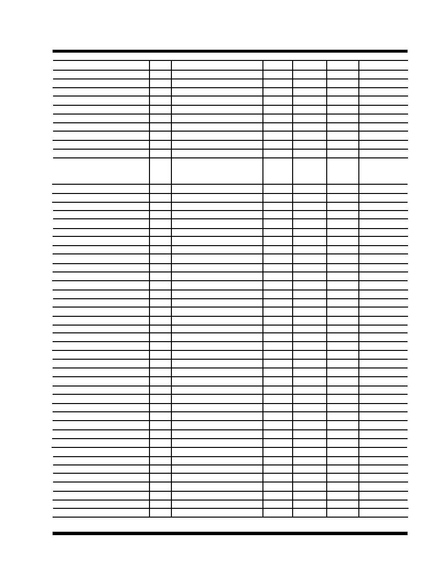
US3018
4-3
Rev. 1.4
12/8/00
Error Comparator Section
Input bias current
2
uA
Input Offset Voltage
-2
+2
mV
Delay to Output
Vdiff=10mV
100
nS
Current Limit Section
C.S Threshold Set Current
200
uA
C.S Comp Offset Voltage
-5
+5
mV
Hiccup Duty Cycle
Css=0.1 uF
10
%
Output Drivers Section
Rise Time
CL=3000pF
70
nS
Fall Time
CL=3000pF
70
nS
Dead band Time Between
High side and Synch Drive
Vcore Switcher Only
CL=3000pF
200
nS
Oscillator Section (internal)
Osc Frequency
200
Khz
2.5V Regulator (Vout 2)
Reference Voltage
Vo2
Ta=25, Vout2 = FB2
1.260
V
Reference Voltage
1.260
V
Dropout Voltage
Io = 200 mA
0.6
V
Load Regulation
1mA< Io <200 mA
0.5
%
Line Regulation
3.1V<Vin2<4V, Vo=2.5V
0.2
%
Input bias current
2
uA
Output Current
200
mA
Current limit
300
mA
Thermal Shutdown
145
�
C
1.5V Regulator (Vout 3)
Reference Voltage
Vo3
Ta=25, GATE3 = FB3
1.260
V
Reference Voltage
1.260
V
Input bias current
2
uA
Output Drive Current
50
mA
Power Good Section
Core U.V lower trip point
Vsen1 ramping down
0.90Vs
V
Core U.V upper trip point
Vsen1 ramping up
0.92Vs
V
Core U.V Hysterises
.02Vs
V
Core O.V upper trip point
Vsen1 ramping up
1.10Vs
V
Core O.V lower trip point
Vsen1 ramping down
1.08Vs
V
Core O.V Hysterises
.02Vs
V
FB2 lower trip point
FB2 ramping down
0.95
V
FB2 upper trip point
FB2 ramping up
1.05
V
FB3 lower trip point
FB3 ramping down
0.95
V
FB3 upper trip point
FB3 ramping up
1.05
V
Power Good Output LO
RL=3mA
0.4
V
Power Good Output HI
RL=5K pull up to 5V
4.8
V
Fault (Overvoltage) Section
Core O.V upper trip point
Vsen1 ramping up
1.17Vs
V
Core O.V lower trip point
Vsen1 ramping down
1.15Vs
V
Vin2 upper trip point
Vin2 ramping up
4.3
V
Vin2 lower trip point
Vin2 ramping down
4.2
V
FAULT Output HI
Io=3mA
10
V
Soft Start Section
Pull up resistor to 5V
OCset=0V , Phase=5V
23
K
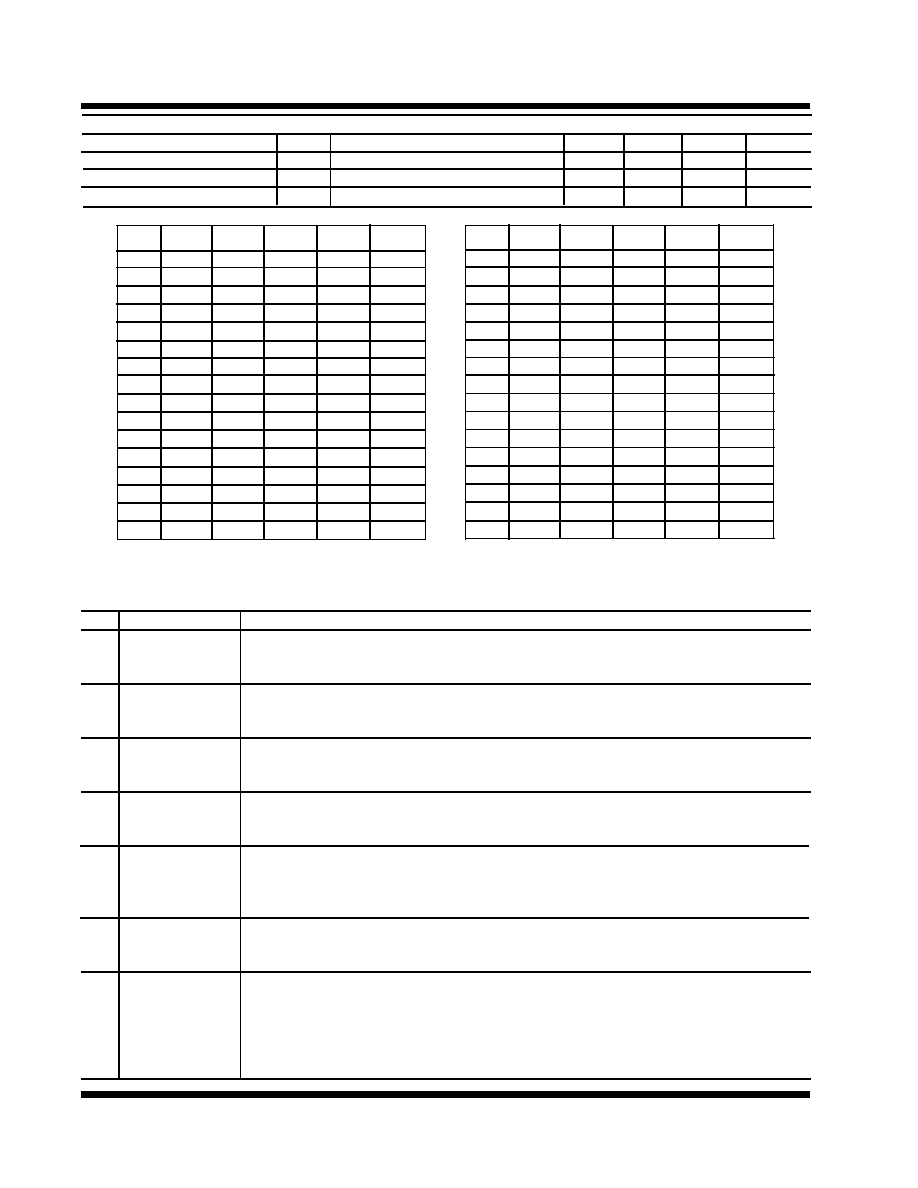
Note 1: Vs refers to the set point voltage given in Table 1.
4-4
Rev. 1.4
12/8/00
US3018
Pin Description
LSB input to the DAC that programs the output voltage. This pin is TTL compatible that
realizes a logic "1" as either HI or Open. When left open,his pin is pulled up internally
by a 27k
resistor to 5V supply.
Input to the DAC that programs the output voltage. This pin is TTL compatible that
realizes a logic "1" as either HI or Open. When left open,his pin is pulled up internally
by a 27k
resistor to 5V supply.
Input to the DAC that programs the output voltage. This pin is TTL compatible that
realizes a logic "1" as either HI or Open. When left open,his pin is pulled up internally
by a 27k
resistor to 5V supply.
MSB input to the DAC that programs the output voltage. This pin is TTL compatible
that realizes a logic "1" as either HI or Open. When left open,his pin is pulled up
internally by a 27k
resistor to 5V supply.
This pin selects a range of output voltages for the DAC.When in the LOW state the
range is 1.3V to 2.05V and when it switches to HI state the range is 2.0V to 3.5V. This
pin is TTL compatible that realizes a logic "1" as either HI or Open. When left open,his
pin is pulled up internally by a 27k
resistor to 5V supply.
This pin is an open collector output that switches LO when any of the outputs are
outside of the specified under voltage trip point. It also switches low when Vsen1 pin is
more than 10% above the DAC voltage setting.
This pin provides the feedback for the synchronous switching regulator. Typically this
pin can be connected directly to the output of the switching regulator. However, a
resistor divider is recommended to be connected from this pin to vout1 and GND to
adjust the output voltage for any drop in the output voltage that is caused by the trace
resistance. The value of the resistor connected from Vou1 to FB1 must be less than
100
.
PIN# PIN SYMBOL
6
VID0
5
VID1
4
VID2
3
VID3
2
VID4
7
PGOOD
18
FB1
PIN DESCRIPTIONS
PIN DESCRIPTIONS
D4
D3
D2
D1
D0
Vs
D4
D3
D2
D1
D0
Vs
0
1
1
1
1
1.30
1
1
1
1
1
2.0
0
1
1
1
0
1.35
1
1
1
1
0
2.1
0
1
1
0
1
1.40
1
1
1
0
1
2.2
0
1
1
0
0
1.45
1
1
1
0
0
2.3
0
1
0
1
1
1.50
1
1
0
1
1
2.4
0
1
0
1
0
1.55
1
1
0
1
0
2.5
0
1
0
0
1
1.60
1
1
0
0
1
2.6
0
1
0
0
0
1.65
1
1
0
0
0
2.7
0
0
1
1
1
1.70
1
0
1
1
1
2.8
0
0
1
1
0
1.75
1
0
1
1
0
2.9
0
0
1
0
1
1.80
1
0
1
0
1
3.0
0
0
1
0
0
1.85
1
0
1
0
0
3.1
0
0
0
1
1
1.90
1
0
0
1
1
3.2
0
0
0
1
0
1.95
1
0
0
1
0
3.3
0
0
0
0
1
2.00
1
0
0
0
1
3.4
0
0
0
0
0
2.05
1
0
0
0
0
3.5
Table 1 - Set point voltage vs. VID codes
Enable Section
En pin input LO voltage
Venl
Regulator OFF
0.8
V
En pin input HI voltage
Venh
Regulator ON
2
V
En pin input LO current
Ven=0V to 0.8V
0.01
uA
En pin input HI current
Ven=2V to 5V
20
uA
US3018
4-5
Rev. 1.4
12/8/00
Pin Description
This pin is internally connected to the undervoltage and overvoltage comparators sensing
the Vcore status. It must be connected directly to the Vcore supply.
This pin is the input that provides power for the internal LDO regulator. It is also monitored
for the under voltage and over voltage conditions.
This pin is connected to the Drain of the power MOSFET of the Core supply and it
provides the positive sensing for the internal current sensing circuitry. An external resis-
tor programs the C.S threshold depending on the Rds of the power MOSFET. An external
capacitor is placed in parallel with the programming resistor to provide high frequency
noise filtering.
This pin is connected to the Source of the power MOSFET for the Core supply and it
provides the negative sensing for the internal current sensing circuitry.
This pin provides the soft start for the switching regulator. An internal resistor charges an
external capacitor that is conected from 5V supply to this pin which ramps up the outputs
of the switching regulators, preventing the outputs from overshooting as wellas limiting
the input current. The second function of the Soft Start cap is to provide long off time
(HICCUP) for the synchronous MOSFET during current limiting.
This pin has dual function. It acts as an output of the OVP circuitry or it can be used to
program the frequency using an external resistor . When used as a fault detector, if the
switcher output exceed the OVP trip point, the FAULT pin switches to 12V and the soft
start cap is discharged. If the FAULT pin is to be connected to any external circuitry, it
needs to be buffered as shown in the application circuit.
This pin controls the gate of an external transistor for the 1.5V GTL+ linear regulator.
This pin provides the feedback for the linear regulator that its output drive is GATE3.
This pin is the output of the internal LDO regulator.
This pin provides the feedback for the internal LDO regulator that its output is Vout4.
This pin serves as the ground pin and must be conected directly to the ground plane.
This pin serves as the Power ground pin and must be conected directly to the GND plane
close to the source of the synchronous MOSFET. A high frequency capacitor (typically 1
uF) must be connected from V12 pin to this pin for noise free operation.
Output driver for the synchronous power MOSFET for the Core supply.
Output driver for the high side power MOSFET for the Core supply.
This pin is connected to the 12 V supply and serves as the power Vcc pin for the output
drivers. A high frequency capacitor (typically 1 uF) must be placed close to this pin and
PGND pin and be connected directly from this pin to the GND plane for the noise free
operation.
5V supply voltage. A high frequency capacitor (0.1 to 1 uF) must be placed close to this
pin and connected from this pin to the GND plane for noise free operation.
This pin is a TTL compatible Enable pin. When this pin is left open or pulled high, the
device is enabled and when is pulled low, it will disable the switcher and the LDO
controller (Vout 3) leaving the internal 200mA regulator operational. When signal is
given to enable the device, both switcher and Vout 3 will go through soft start, the
same as during start up.
PIN# PIN SYMBOL
19
VSEN1
12
VIN2
20
OCSET1
23
PHASE1
9
SS
10
FAULT/Rt
15
GATE3
16
FB3
13
VOUT2
11
FB2
14
GND
21
PGND
22
LGATE1
24
UGATE1
1
V12
8
V5
17
En