US3033
4-1
Rev. 1.5
1/14/99
PWM SWITCHER & LINEAR
CONTROLLER IC
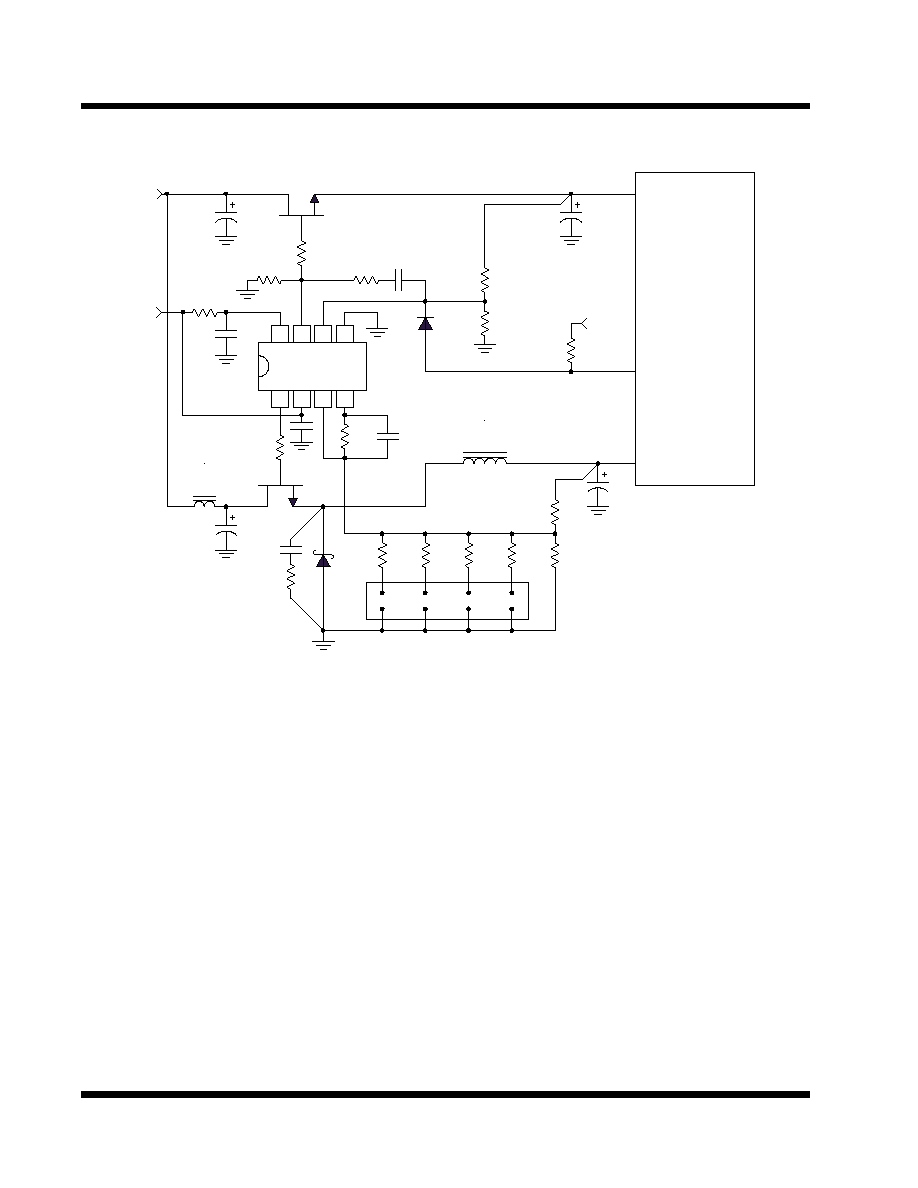
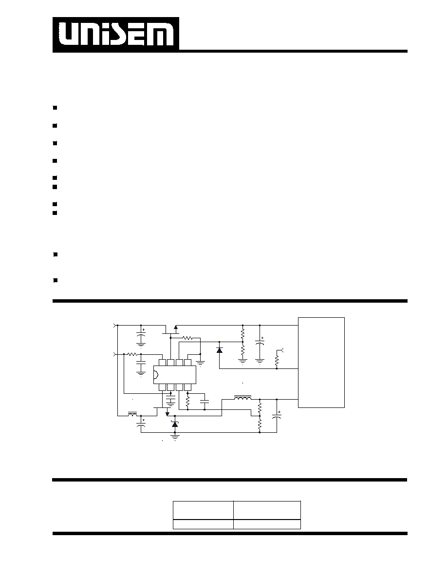
TYPICAL APPLICATION
TYPICAL APPLICATION
Typical application of US3033 in a flexible mother board designed for Intel P55
TM
,P54
TM
AMD K5,K6
TM
as well as Cyrix M1
TM
and M2
TM
applications.
TA (∞C) 8 PIN PLASTIC
SOIC (S)
0 TO 70 US3033CS
Notes: P54C,P55C,Pentium II are trade marks of Intel Corp. K5 & K6 are trade marks of AMD corp. Cyrix 6X86L,M1,M2 are trade marks
of Cyrix Corp. Power PC is trade mark of IBM Corp.
DESCRIPTION
DESCRIPTION
The US3033 IC combines a switching controller and
a linear regulator controller all in a compact 8 pin
surface mount package, providing a total solution for
dual supply processor applications such as an Intel
P55C
TM
, AMD K6
TM
, as well as Cyrix 6X86L
TM
and
the M2
TM
processors. Typically in these applications a
dual supply regulator converts 5V to 3.3V for I/O supply
and a jumper programmable supply of 1.25V to 3.5V for
CORE supply .The linear regulator controller portion in
the US3033 is a programmable controller allowing flex-
ibility for the I/O regulator and has a minimum of 50mA
drive current capability designed to provide ample cur-
rent for an external pass transistor. The IC uses an inter-
nal regulator generated from the 12V supply to power
the controller as well as the 12V supply to drive the power
MOSFET, allowing a low cost N channel MOSFET
switch to be used. The IC also includes an error com-
parator for fast transient response, a precise voltage ref-
erence for setting the output voltage as well as a direct
drive of the MOSFET for the minimum part count.
FEATURES
FEATURES
LDO Controller allows the use of a low cost
pass transistor for the I/O supply
8 pin SOIC combines switching and linear
controller
Internal Pre-regulator Eliminates Cross talk
between Switching & Linear regulators
Automatic shut down of the linear regulator
when connected to the Vcc2 Det pin
On board MOSFET driver
Fastest transient response of any controller
method. ( 0 to 100% Duty Cycle in 100 nS )
1% internal voltage reference
Internal Under Voltage Lockout protects
MOSFET during start-up
APPLICATIONS
APPLICATIONS
Dual supply low voltage processor applications,
such as: P55C
TM
,CYRIX M2
TM
, POWER PC
TM
and
AMD K6
TM
Simple 5V to 3.3V switcher for Pentium with AGP
or Pentium II
TM
applications
PACKAGE ORDER INFORMATION
PACKAGE ORDER INFORMATION
3033app1-1.1
CPU
I / O
Vcc2 Det
Core
5V
5V
12V
Q1
C1
L1
C3
Q2
D1
C2
L2
R4
R5
C7
R6
R7
C6
R8
R3
C5
1
2
3
4
5
6
7
8
Drv1V12swVfb1 Vhyst
Gnd
Vfb2
Drv2
V12
US3033
D2
R10
C8
R9
US3033
4-2
Rev. 1.5
1/14/99
ABSOLUTE MAXIMUM RATINGS
ABSOLUTE MAXIMUM RATINGS
V
12
,V
12SW
Supply Voltages ............................................................. 20V
F.B Pin Voltages........................................................ -0.3V to 5V
Storage Temperature Range ................................. -65 TO 150
∞
C
Operating Junction Temperature ............................... 0 TO 150
∞
C
PACKAGE INFORMATION
PACKAGE INFORMATION
8 PIN PLASTIC SOIC (S)
JA
=160
∞
C/W
Linear Controller Section
PARAMETER
SYM
TEST CONDITION
MIN TYP MAX UNITS
F.B Voltage Initial Accuracy V
FB2
T
J
=25
∞
C, Drv2=V
FB2
, C
L
=100uF
1.237
1.250
1.262
V
F.B Voltage Total Variation
Drv2=V
FB2
, C
L
=100uF
1.225
1.250
1.275
V
F.B Voltage Line Regulation
10<V
12
<14V,Drv2=V
FB2
, C
L
=100uF
0.2
%
F.B Input Bias Current
I
FB2
V
FB2
=1.25V
-1
+1
uA
Maximum Drive Current I
DRVMAX
V
FB2
=1V, V
FB1
=1.5V
50
mA
V
12
Supply Current
I
12
V
FB2
=1V, V
FB1
=1.5V, I
DRV2
=0
5
mA
Switching Controller Section
PARAMETER
SYM TEST CONDITION
MIN TYP MAX UNITS
F.B Voltage Initial Accuracy
V
FB1
T
J
=25
∞
C
1.237
1.250
1.262
V
F.B Voltage Total Variation
1.225
1.250
1.275
V
F.B Voltage Line Regulation
0.2
%
F.B Input Bias Current
I
FB1
V
FB1
=1.25V
-1
+1
uA
Min On Time
V
FB1
is sq wave with 300 ns on
800
nS
time and 2 uS off time
Min Off Time
V
FB1
is sq wave with 300 ns off
800
nS
time and 2 uS on time
Vhyst pin output-HI
I
SOURCE
=500uA, V
FB1
=1.5V
11
V
Vhyst pin output-LO
I
SINK
=500uA, V
FB1
=1V
1
V
Supply Current
I
12SW
V
FB1
=1V , V
FB2
=1.5V
10
mA
Maximum Duty Cycle
D
MAX
V
FB1
=1V
100
%
Minimum Duty Cycle
D
MIN
V
FB1
=1.5V
0
%
Gate Drive Rise/Fall Time
V
GATE
Load=IRL3303
70
nS
ELECTRICAL SPECIFICATIONS
ELECTRICAL SPECIFICATIONS
Unless otherwise specified the following specification applies over V
12
=V
12SW
=12V, and T
A
=0 to 70
∞
C. Low duty
cycle pulse testing are used which keeps junction and case temperatures equal to the ambient temperature.
4
3
2
1
5
6
7
8
TOP VIEW
Drv1
V12sw
Vfb1
Vhyst
Gnd
Vfb2
Drv2
V12
US3033
4-5
Rev. 1.5
1/14/99
Ref Desig
Description Qty
Part #
Manufacturer
U1
LDO/Switcher IC
1
US3033CS ( 8 pin SOIC)
Unisem
Q1
MOSFET
1
MTP3055 (TO220)
Motorola
Q2
MOSFET
1
IRL3303 (TO220)
International
IRL3103S (TO263) (note 1)
Rectifier
D2
Diode, GP
1
1N4148
D1
Schottky Diode
1
MBR1045CT (TO220)
MBRB1545CT (TO263) (note1)
Motorola
L2
Inductor
1
Core:T50-18,L=4 uH
Micro Metal
Turns: 10T, 18 AWG
(core)
L1
Inductor
1
L=2 uH
R1
Resistor
1
22 ohm,5%, SMT 1206 size
R2
Resistor
1
10 ohm, 5%, SMT 1206 size
R3
Resistor
1
324 kohm,1%, SMT 0805 size
R4A *
Resistor
1
806 ohm,1%, SMT 0805 size
R4B *
Resistor
1
90.9 kohm,1%, SMT 0805 size
R5A
Resistor
1
1.24 kohm,1%, SMT 0805 size
R5B
Resistor
1
2.49 kohm,1%, SMT 0805 size
R5C
Resistor
1
4.99 kohm,1%, SMT 0805 size
R5D
Resistor
1
10 kohm,1%, SMT 0805 size
R5E
Resistor
1
1.30 kohm,1%, SMT 0805 size
R6
Resistor
1
2k ohm,1%, SMT 0805 size
R7
Resistor
1
1.21k ohm,1%, SMT 0805 size
R8
Resistor
1
1 kohm,5%, SMT 0805 size
R9
Resistor
1
10 ohm,5%, SMT 0805 size
R10
Resistor
1
1k ohm,5%, SMT 0805 size
R11
Resistor
1
2.4k ohm,5%, SMT 0805 size
R13
Resistor
1
7.5k ohm,5%, SMT 0805 size
C1
Capacitor
1
6MV1500GX, 1500uF,6.3V, Elect
C2
Capacitor
1
6MV1500GX, 1500uF,6.3V, Elect
Sanyo
C3
Capacitor
1
1 uF,Ceramic, SMT 0805 size
C4
Capacitor
1
470 pF,Ceramic, SMT 0805 size
Sanyo
C5
Capacitor
1
10 pF,Ceramic, SMT 0805 size
Sanyo
C6
Capacitor
1
6MV1500GX, 1500uF,6.3V, Elect
Sanyo
C7
Capacitor
4
6MV1500GX, 1500uF,6.3V, Elect
Sanyo
C8
Capacitor
1
1 uF,Ceramic, SMT 0805 size
C9
Capacitor
1
470pF ,Ceramic, SMT 0805 size
HS1
Heat Sink
1
For MOSFET , 577002
Aavid
HS2
Heat Sink
1
For Schottky Diode , 577002
Aavid
HS3
Heat Sink
1
For Q1 , 507222 (I/O curren<5A)
Aavid
576602 (I/O current< 3.5A)
* R4 is a parallel combination of R4A and R4B.
Note 1: For the applications where it is desirable to eliminate the heat sink, the IRL3103S for Q2 and MBR1545CT for D2 in TO263
packages with minimum of 1" square copper pad can be used.
Pentium Dual Supply Application Parts List