SIDE LOOK PACKAGE
NPN PHOTOTRSNSISTOR
MID-13A45
Description
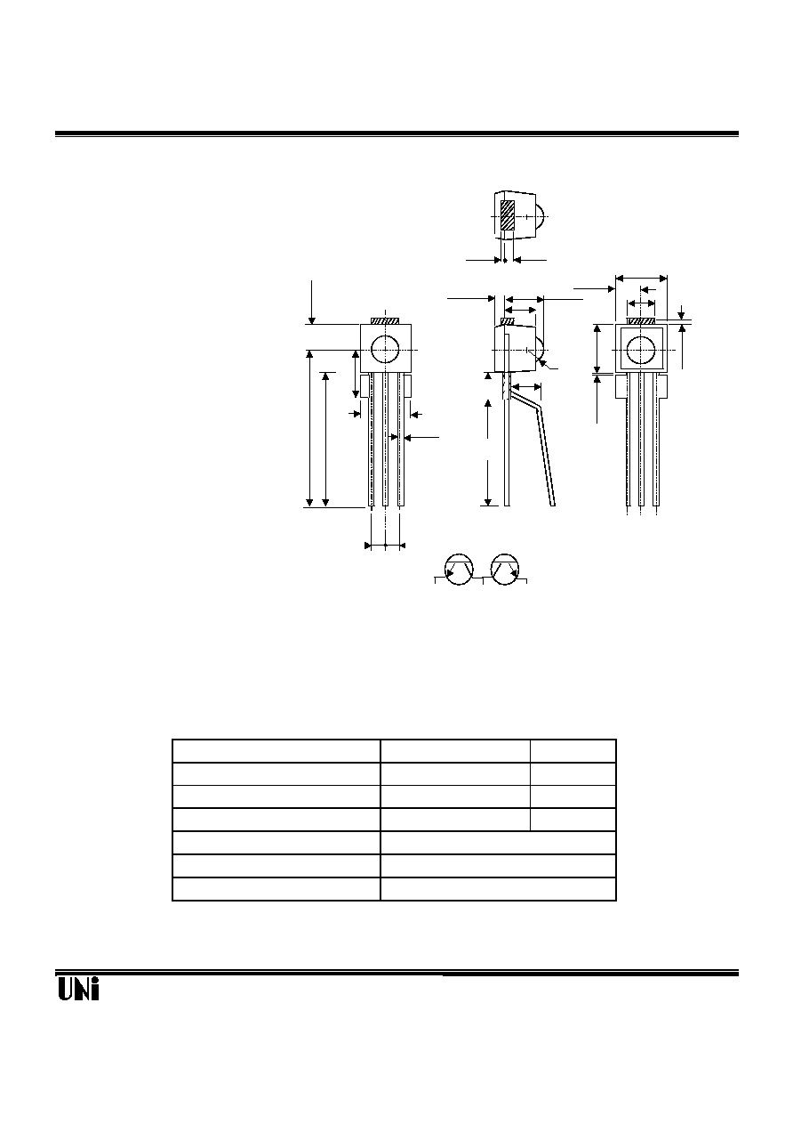
Package Dimensions
The MID-13A45 is a Two Bits silicon phototransistor
mounted in a special dark plastic side looking package.
The lensing effect of the package allows a wide accep-
tance angle.
Features
l
Wide range of collector current
l
Low cost plastic package
l
High resolution for mouse application
Absolute Maximum Ratings
@ T
A
=25
o
C
Parameter
Maximum Rating
Unit
Power Dissipation
100
mW
Collector-Emitter Voltage
30
V
Emitter-Collector Voltage
5
V
Operating Temperature Range
Storage Temperature Range
Lead Soldering Temperature
02/04/2002
-55
o
C to +100
o
C
-55
o
C to +100
o
C
260
o
C for 5 seconds
Unity Opto Technology Co., Ltd.
NOTES :
1. All dimensions are in millimeters.(inches).
2. Tolerance is ± 0.25mm (.010") unless otherwise noted .
3. Lead spacing is measured where the leads emerge from the package.
Unit: mm(inches)
.50MAX
(.020)MAX
.30MAX
(.012)MAX
2.30 ± .30
(.091±.012)
1.70 ± .10
(.067±.004)
7.60
(.299)
9.60
(.378)
1.25
(.049)
1.25
(.049)
3*0.5
3.90
+0
-.20
3.70 ± .10
(.146±.004)
2.00MAX(.079)MAX
2.00 ± .10
(.079±.004)
4.00 ±.10
(.158±.004)
.25MAX
(.010)MAX
2.45 ±.10
(.097±.004)
.80 ± .10
(.032±.004)
2.05
(.081)
R1.1
4.00 ± .10
(.158±.004)
2.00
(.079)
5.60
(.221)
.25MAX
(.010)MAX
1
2
3
1
2
3
EMITTER (PTR A)
COLLECTOR(COM)
EMITTER (PTR B)
1
2
3

MID-13A45
Optical-Electrical Characteristics
@ T
A
=25
o
C
Parameter
Test Conditions
Symbol
Min.
Typ .
Max.
Unit
Collector-Emitter
I
c
=0.1mA
V
(BR)CEO
30
V
Breakdown Voltage
Ee=0
Emitter-Collector
Ie=0.1mA
V
(BR)ECO
5
V
Breakdown Voltage
Ee=0
Collector-Emitter
I
c
=0.5mA
V
CE(SAT)
0.1
0.4
V
Saturation Voltage
Ee=0.1mW/cm
2
Rise Time
V
R
=5V , R
L
=1K
Tr
10
µ
S
Fall Time
I
C
=1mA
Tf
10
Collector Dark
V
CE
=10V
I
CEO
100
nA
Current
Ee=0
On State Collector
V
CE
=5V
I
C(ON)
0.16
0.4
mA
Current
Ee=0.1mW/cm
2
Typical Optical-Electrical Characteristic Curves
02/04/2002
Unity Opto Technology Co., Ltd.
0.001
0.01
0.1
1
10
100
1000
0
40
80
120
T
A
- Ambient Temperature -
o
C
FIG.1 COLLECTOR DARK CURRENT
VS AMBIENT TEMPERATURE
0
4
8
12
16
20
0
2
4
6
8
10
Vcc = 5 V
V
RL
= 1 V
F = 100 Hz
PW = 1
µ
s
R
L
- Load Resistance - K
FIG.3 RISE AND FALL TIME
VS LOAD RESISTANCE
0.0
0.4
0.8
1.2
1.6
2.0
0
0.1
0.2
0.3
0.4
0.5
0.6
Vce = 5 V
Ee - Irradiance - mW/cm
2
FIG.4 RELATIVE COLLECTOR CURRENT
VS IRRADIANCE
0.0
0.5
1.0
1.5
2.0
2.5
3.0
3.5
4.0
-75
-25
25
75
125
Vce = 5 V
Ee = 0.1 mW/cm
2
@
= 940 nm
T
A
- Ambient Temperature -
o
C
FIG.2 NORMALIZED COLLECTOR CURRENT
VS AMBIENT TEMPERATURE
Relative Collector Current (mA)
Tr Tf - Rise and Fall Time -
µ
S
Iceo-Collector Dark Current -
µ
A
I
C
Normalized Collector Current