T-1 3/4 PACKAGE
NPN PHOTOTRANSISOR
MID-52A22
Description
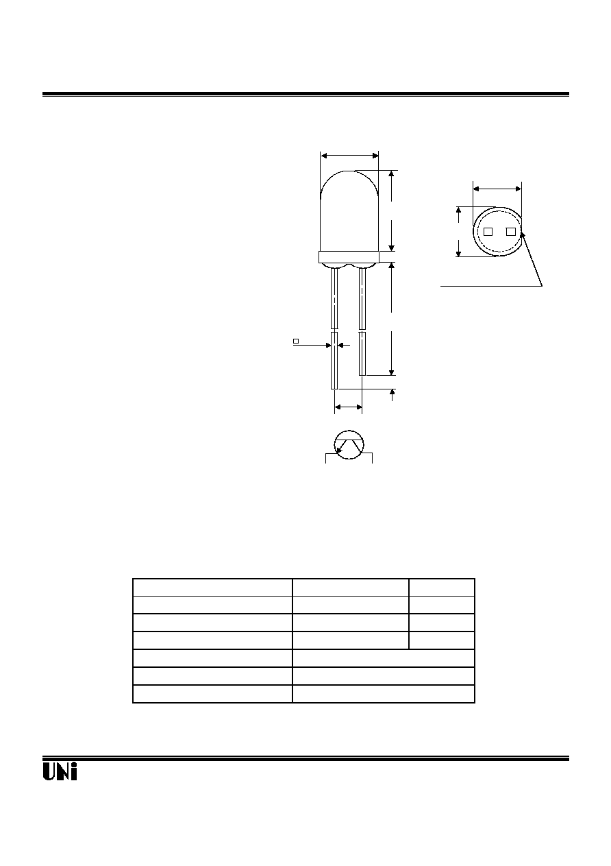
Package Dimensions
The MID-52A22 is a NPN silicon phototransistor mounted
in a lensed, special dark plastic package. The lensing effect
of the package allows an acceptance view angle of 20
o
so
that the product performs a high directional characteristic.
Features
l
Wide range of collector current
l
Lensed for high sensitivity
l
Low cost plastic package
l
Standard T-1 3/4 (5mm) package.
l
Good spectral matching IRED (940nm) type.
l
Acceptance angle :20
o
Absolute Maximum Ratings
@ T
A
=25
o
C
Parameter
Maximum Rating
Unit
Power Dissipation
150
mW
Collector-Emitter Voltage
30
V
Emitter-Collector Voltage
5
V
Operating Temperature Range
Storage Temperature Range
Lead Soldering Temperature
02/04/2002
-55
o
C to +100
o
C
-55
o
C to +100
o
C
260
o
C for 5 seconds
Unity Opto Technology Co., Ltd.
Unit : mm (inches )
Notes :
1.Tolerance is ± 0.25 mm (.010") unless otherwise noted.
2.Protruded resin under flange is 1.0 mm (.040") max.
3.Lead spacing is measured where the leads emerge from the package.
5.05
(.200)
2.54
(.100)
7.62
(.300)
1.00
(.040)
0.50TYP.
(.020)
1.00MIN.
(.040)
FLAT DENOTES COLLECTOR
5.47
(.215)
5.90
(.230)
23.40MIN.
(.920)
C
E

MID-52A22
Optical-Electrical Characteristics
@ T
A
=25
o
C
Parameter
Test Conditions
Symbol
Min.
Typ .
Max.
Unit
Collector-Emitter
I
c
=0.1mA
Breakdown Voltage
Ee=0
Emitter-Collector
Ie=0.1mA
Breakdown Voltage
Ee=0
Collector-Emitter
I
c
=0.5mA
Saturation Voltage
Ee=0.1mW/cm
2
Rise Time
V
cc
=5V , R
L
=1K
Tr
15
Fall Time
I
C
=1mA
Tf
15
Collector Dark
V
CE
=10V
Current
Ee=0
On State Collector
V
CE
=5V
Current
Ee=0.1mW/cm
2
Typical Optical-Electrical Characteristic Curves
02/04/2002
I
C(ON)
0.8
mA
V
CE(SAT)
nA
100
I
CEO
µ
S
V
V
V
0.4
V
(BR)CEO
V
(BR)ECO
30
5
Unity Opto Technology Co., Ltd.
T
A
- Ambient Temperature -
o
C
FIG.2 NORMALIZED COLLECTOR CURRENT
VS AMBIENT TEMPERATURE
Ee - Irradiance - mW/cm
2
FIG.4 RELATIVE COLLECTOR CURRENT
VS IRRADIANCE
0.001
0.01
0.1
1
10
100
1000
0
40
80
120
T
A
- Ambient Temperature -
o
C
FIG.1 COLLECTOR DARK CURRENT
VS AMBIENT TEMPERATURE
0.0
0.5
1.0
1.5
2.0
2.5
3.0
3.5
4.0
-75
-25
25
75
125
0
40
80
120
160
200
0
2
4
6
8
10
R
L
- Load Resistance - K
FIG.3 RISE AND FALL TIME
VS LOAD RESISTANCE
0
1
2
3
4
5
0 0.1 0.2 0.3 0.4 0.5 0.6
Vce = 5 V
Relative Collector Current (mA)
I
C
Normalized Collector Current
Vcc = 5 V
V
RL
= 1 V
F = 100 Hz
PW = 1 ms
Tr Tf Rise and Fall Time -
µ
S
Iceo-Collector Dark Current -
µ
A
FIG .5 SENSITIVITY DIAGRAM
1.0
0.9
0.8
0∞ 10∞ 20∞
0.5 0.3 0.1 0.2 0.4 0.6
Relative Sensitivity
Vce = 5 V
Ee = 0.1 mW/cm
2
@
= 940 nm
40∞
90∞
70∞
60∞
50∞
80∞
30∞