SUBMINIATURE
PHOTOINTERRUPTER
Description
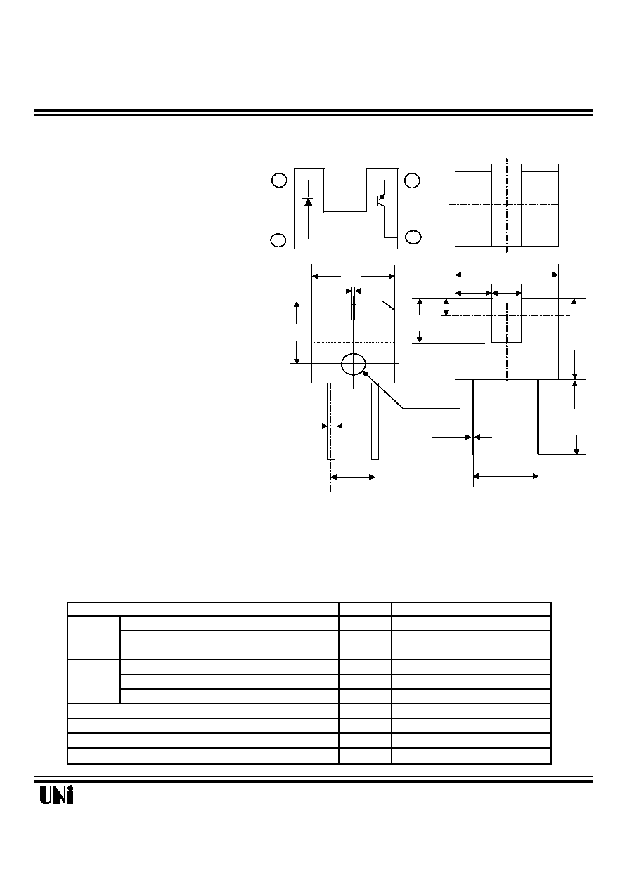
Package Dimensions
Unit : mm
The MIT-4A11B consists of a Gallium Arsenide in-
frared emitting diode and a NPN silicon phototran-
sistor , double-layer mold plastic package. It is a
transmissive subminiature photointerrupter.
Features
l
Ultra-compact
`
l
PWB mounting type package
l
High sensing accuracy ( Slit width: 0.3mm )
l
Gap between light emitter and detector: 1.2mm
Applications
l
Cameras
l
Floppy disk drives
l
Printer
NOTE
1. Tolerance is ± 0.25 mm (.010") unless otherwise noted.
2. Burr's dimension : 0.15MAX
3.( ) : Reference dimensions
4. The dimensions indicated by * refer to those measured
Absolute Maximum Ratings
from the lead base
Parameter
Symbol
Maximum Rating
Unit
Continuous Forward Current
I
F
50
mA
INPUT
Reverse Voltage
V
R
5
V
Power Dissipation
P
ad
75
mW
Collector-emitter breakdown voltage
V
(BR)CEO
30
V
OUTPUT Emitter-Collector breakdown voltage
V
(BR)ECO
5
V
Collector power dissipation
P
C
75
mW
Total power dissipation
P
TOT
mW
Operating Temperature Range
T
opr
Storage Temperature Range
T
stg
Soldering temperature
T
sol
MIT-4A11B
01/30/2002
-25 to + 85
-40 to + 100
100
260
o
C for 3 seconds
Unity Opto Technology Co., Ltd.
@T
A
=25
1
2
3
4
A
C
C
E
5.2
4.0
MIN.
4-0.15
*3.2
*2.54
3.9
2.8
1.5
1.2
4.2
4.2
(1.0)
1.5±0.1Hold ±
(0.3)
4-0.5
MIT-4A11B
Optical-Electrical Characteristics
Parameter
symbol
Min.
Typ.
Max.
Unit.
Test Conditions
Input
Forward Voltage
V
F
1.2
1.4
V
I
F
=20mA
Reverse Current
I
R
10
µ
A
V
R
=3V
Collector Dark Current
Iceo
100
nA
Vce =10V
V
CE(SAT)
0.4
V
Ic=0.1mA,Ee=0.1mW/cm
2
Collector Current
Ic (on)
0.6
5.0
mA
I
F
=20mA, Vce =5V
Transfer Cha- Response Time (RISE)
t
r
50
150
µ
S
racteristics
Response Time (FALL)
t
f
50
150
µ
S
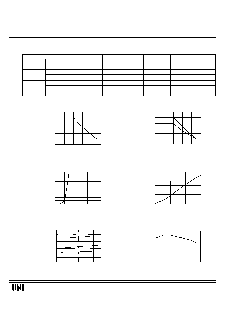
Typical Optical-Electrical Characteristic Curves
Collector Emitter Saturation Voltage
01/30/2002
Ic=100
µ
A, Vce =5V
R
L
=1K
@T
A
=25
Unity Opto Technology Co., Ltd.
0
5
10
15
20
25
30
0
20
40
60
80
100
120
-25
0
25
50
75
100
Ambient Temperature T
A
(
o
C )
Fig.2 Power Dissipation vs
Ambient Temperature
Power Dissipation (mW)
P
TOT
P
D
, P
C
0
20
40
60
80
100
120
-25
0
25
50
75
100
Collector Current Ic (mA)
Vce=2V
Ta=25
Forward Current I
F
(mA)
Fig.4 Collector Current vs
Forward Current
0
10
20
30
40
50
60
-25
0
25
50
75
100
Ambient Temperature T
A
Fig.1 forward Current
VS
.
Ambient Temperature
Relative Collector Current (%)
Ambient Temperature T
A
(
o
C )
Fig.6 Relative Collector Current
VS
. T
A
Forward Current I
F
(mA)
Forward Current I
F
(mA)
Output
Forward Voltage V
F
(V)
Fig.3 Forward Current
VS
Forward Voltage
0
2
4
6
8
10
12
Collector-Emitter Voltage Vce (V)
Fig.5 Collector Current vs. Vce
Ta=25
Collector Current Ic (
m
A)
I
F
=15mA
10mA
4mA
20mA
0
0.4
0.8
1.2
1.6
2.0
2.4
2.8
0
0.4
0.8
1.2
1.6
2.0
2.4
2.8
0
20
40
60
80
100
0.8
1.2
1.6
2.0
2.4
2.8
MIT-4A11B
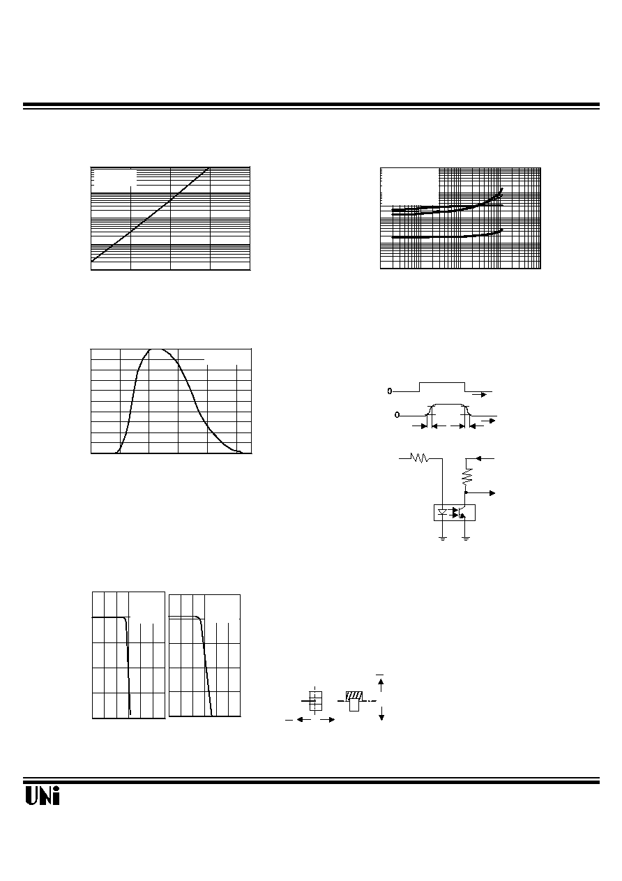
Typical Optical-Electrical Characteristic Curves
Response Time Measurement Circuit
Sensing Position Characteristics
(Typical)
(Center of optical axis)
01/30/2002
1
10
100
1000
10000
0
25
50
75
100
0.1
1
10
100
1000
0.01
0.1
1
10
100
V
CE
=20V
V
CE
=2V
I
C
=100
µ
A
Ta=25
Response Time (
µ
s)
Load Resistance R
t
(K
)
Fig.8 Response Time vs.
Load Resistance
Collector Dark Current I
CEO
Unity Opto Technology Co., Ltd.
0
20
40
60
80
100
700
800
900
1000
1100
1200
Relative Sensitivity (%)
Wavelength (nm)
Fig.9 Spectral Sensitivity (Detecting side)
Ambient Temperature T
A
( )
Fig.7 Collector Dark Current vs.
Ambient Temperature
Ta=25
Input
Output
90 %
10 %
tr
tf
t
t
0
50
100
-2 -1 0 +1 +2 (mm) -2 -1 0 +1 +2 (mm)
Relative light current I
L
(%)
I
F
=20mA
V
CE
=5V
Ta=25
I
F
=20mA
V
CE
=5V
Ta=25
Distance d (mm)
Y
X
0
+
0
+
Y
X
IL
Input
V
CC
Output
VR