GPTR3190
PHASE CONTROLLED SCR
High reliability operation
DC power supply
AC drives
VOLTAGE UP TO
2400 V
AVERAGE CURRENT
1900 A
SURGE CURRENT
22 kA
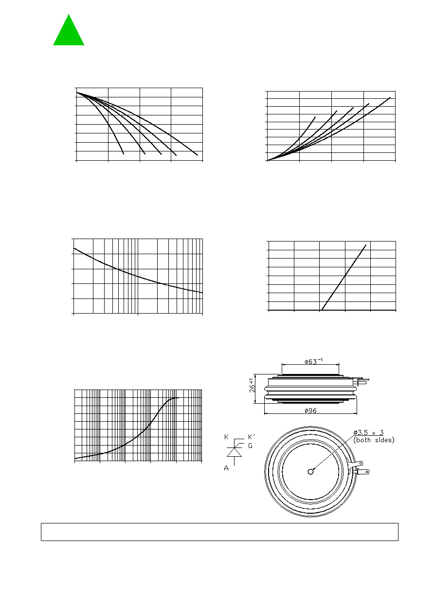
BLOCKING CHARACTERISTICS
Characteristic
Conditions
V
RRM
Repetitive peak reverse voltage
2400 V
V
RSM
Non-repetitive peak reverse voltage
2500 V
V
DRM
Repetitive peak off-state voltage
2400 V
I
DRM
Repetitive peak off-state current, max.
V
DRM
, single phase, half wave, Tj = Tjmax
70 mA
I
RRM
Repetitive peak reverse current, max.
V
RRM
, single phase, half wave, Tj = Tjmax
70 mA
ON-STATE CHARACTERISTICS
I
T(AV)
Average on-state current
Sine wave,180∞ conduction, Th = 55 ∞C
1900 A
I
T(RMS)
R.M.S. on-state current
Sine wave,180∞ conduction, Th = 55 ∞C
2984 A
I
TSM
Surge on-state current
Non rep. half sine wave, 50 Hz, V
R
= 0 V, T
j
= T
jmax
22 kA
I≤t
I≤ t for fusing coordination
2420 kA≤s
V
T(TO)
Threshold voltage
T
j
= T
jmax
1.04 V
r
T
On-state slope resistance
T
j
= T
jmax
0.23 m
V
TM
Peak on-state voltage, max
On-state current I
T
= 5000 A , Tj = 25 ∞C
2.15 V
I
H
Holding current, max
T
j
= 25 ∞C
300 mA
I
L
Latching current, typ
T
j
= 25 ∞C
500 mA
TRIGGERING CHARACTERISTICS
V
GT
Gate trigger voltage
T
j
= 25 ∞C, V
D
= 5 V
3 V
I
GT
Gate trigger current
T
j
= 25 ∞C, V
D
= 5 V
400 mA
V
GD
Non-trigger voltage
V
D
= 67% V
RRM
, T
j
= T
jmax
0.15 V
P
GM
Peak gate power dissipation
Pulse width 0.5 ms
100 W
P
G(AV)
Average gate power dissipation
5 W
I
FGM
Peak gate current
30 A
V
FGM
Peak gate voltage (forward)
12 V
V
RGM
Peak gate voltage (reverse)
3 V
SWITCHING CHARACTERISTICS
di/dt
Critical rate of rise of on-state current
T
j
= T
jmax
200 A/µs
dV/dt
Critical rate of rise of off-state voltage
T
j
= T
jmax
1000 V/µs
t
q
Turn-off time, typ
T
j
= T
jmax
, I
T
= 800 A, di/dt = -12.5 A/µs
400 µs
VR = 100 V, VD = 67% VDRM, dV/dt = 20 V/µs
THERMAL AND MECHANICAL CHARACTERISTICS
R
th(j-c)
Thermal resistance (junction to case)
Double side cooled
0.016 ∞C/W
R
th(c-h)
Thermal resistance (case to heatsink)
Double side cooled
0.001 ∞C/W
T
jmax
Max operating junction temperature
125 ∞C
T
stg
Storage temperature
-40 / 125 ∞C
F
Clamping force ± 10%
30 kN
Mass
1400 g
Document GPTR3190T001
Value
Green Power Solutions srl
Via Greto di Cornigliano 6R - 16152 Genova , Italy
Phone: +39-010-659 1869
Fax: +39-010-659 1870
Web: www.gpsemi.it
E-mail: info@gpsemi.it
Green Power
Semiconductors