 | –≠–ª–µ–∫—Ç—Ä–æ–Ω–Ω—ã–π –∫–æ–º–ø–æ–Ω–µ–Ω—Ç: LR4102 | –°–∫–∞—á–∞—Ç—å:  PDF PDF  ZIP ZIP |
March 2000
1
Copyright © 1998≠2000 by LSI Logic Corporation. All rights reserved.
TinyRISC
Æ
LR4102
Microprocessor
Datasheet
The TinyRISC LR4102 Microprocessor is a compact, high performance
32-bit microprocessor implemented in the LSI Logic G11TM technology.
The LR4102 is a complete microprocessor solution with caches, an
external bus interface with built-in memory controllers, and on-chip
debug. The LR4102 is built using the EZ4102 EasyMACRO subsystem,
available to customers through the LSI Logic CoreWare
Æ
program.
The LR4102 provides a 32-bit FBusMACRO to control all off-chip data
transactions (including DRAM or SDRAM) and an EJTAG interface for
on-chip debug with PC trace output.
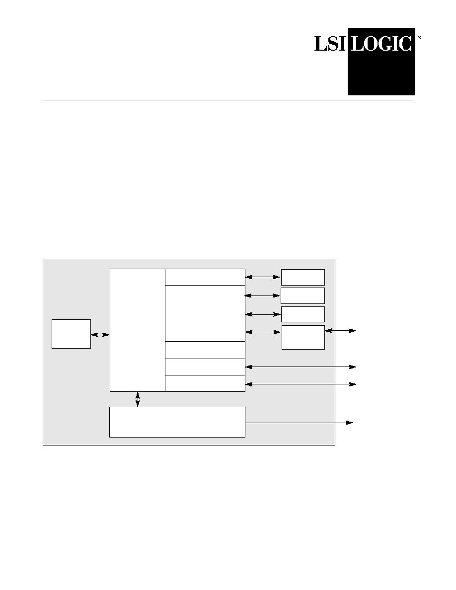
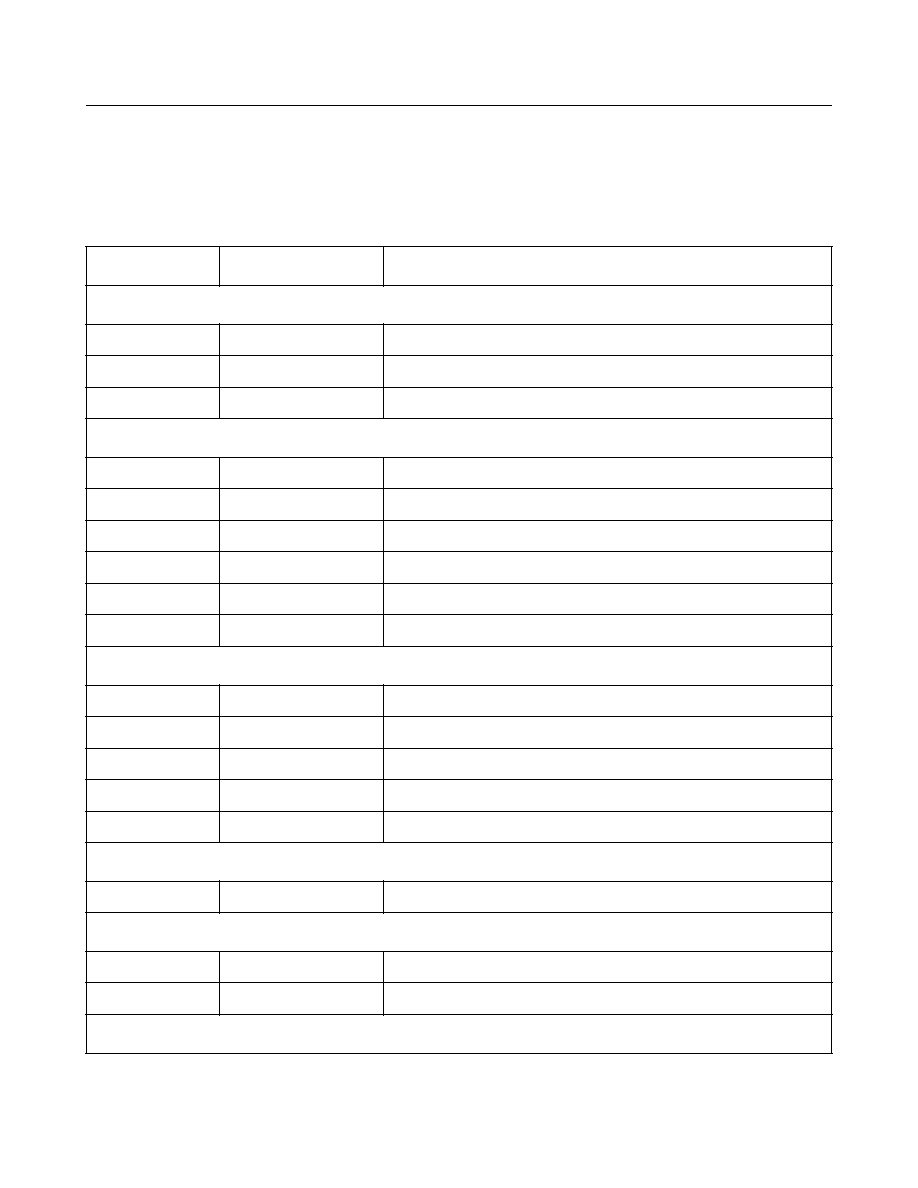
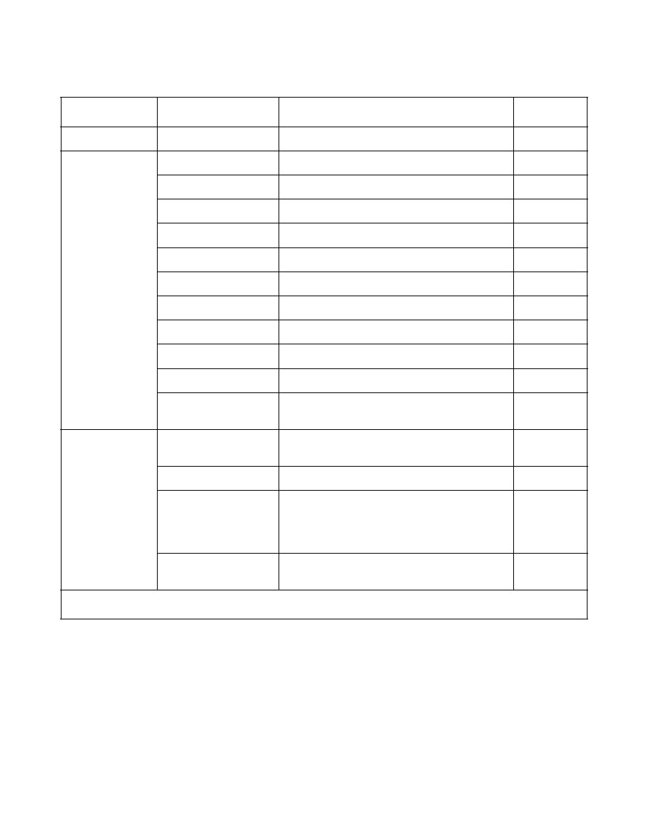
Figure 1
illustrates the LR4102 chip.
Figure 1
LR4102 Block Diagram
The LR4102 microprocessor is powered by either 2.5 V (for 85 MHz
operation) or 1.8 V (for 50 MHz operation). The chip I/O ring requires
3.3 V. With a system clock of 85 MHz, peak performance is 85 MIPS and
sustained performance is estimated at 68 MIPS. With a 50 MHz clock,
performance is 50 MIPS peak and 40 MIPS sustained.
LR4102
Two 32-bit Timers
SerialICETM-1 Port
EJTAG
OCM
EJTAG
SerialICE-1
MMU
BIU and Cache
32-bit TinyRISC
Controller (BBCC)
FBus-
TLB RAM
MACRO
PC Trace
FBus
Clock
Controller
Output
4102 CPU
and FastMDU
Interface
Interface
EJTAG
Caches
Extended Debug MACRO

2
TinyRISC LR4102 Microprocessor
LR4102 Features
Components
∑
R3000 MIPS CPU executes
MIPS II and MIPS16
instructions
∑
32-bit FBus, a fast
demultiplexed multimaster
bus, with built in control of:
≠
RAM, EPROM, or similar
simple devices
≠
DRAM and SDRAM
≠
General-purpose I/O
∑
Two 32-bit Timers
∑
FastMDU
≠
4/5 cycle multiply and
accumulate (32-bit to
64-bit)
≠
34/35 cycle divide
∑
BBCC with four writeback
buffers included
∑
MMU with 64-entry TLB RAM
∑
EJTAG Version 2.0.0:
≠
Nonintrusive debug
≠
Real-time PC trace
≠
Hardware breakpoints
∑
SerialICE-1 Port included for
backward compatibility with
other TinyRISC designs
∑
JTAG Boundary Scan
∑
On-Chip Memory (OCM),
1 Kbyte
∑
Caches
≠
16 Kbytes of two-way
set-associative I-Cache
≠
8 Kbytes of direct-mapped
D-Cache
∑
Clock module with integrated
PLL and programmable clock
speeds
Technology
∑
LSI Logic G11 Technology
≠
0.18
µ
L
eff
(0.25
µ
drawn)
≠
2.5 or 1.8 V operation
Performance and Compatibility
∑
Clock speed is 85 MHz at 2.5 V
(85 MIPS peak and estimated
68 MIPS sustained)
∑
Low power mode allows LR4102
to use minimal power when idle
∑
Compatible with the full range of
MIPS and third-party software
development tools
∑
16-bit and 32-bit code can be
mixed arbitrarily with full support
on a subroutine basis
∑
All instructions execute in one
cycle except for Load and Store,
Move To Coprocessor, and Move
From Coprocessor, which
execute in two cycles, and MDU
instructions, which execute in
several cycles

TinyRISC LR4102 Microprocessor
3
Block Diagram
This section provides short descriptions of the major components of the
LR4102, as shown in
Figure 1
.
The CPU performs all arithmetic, logical, shift, and address calculations.
The CPU supports EJTAG debug and is closely coupled with the
FastMDU. The FastMDU calculates all multiply and divide operations for
the LR4102, and provides 4/5 cycle multiply and accumulate operations
(32 bit to 64 bit), 34/35 cycle divide, saturated math, and overflow
indication.
The memory management unit (MMU) translates virtual addresses from
the CPU into physical addresses and includes a 64-entry translation
look-aside buffer (TLB) RAM.
The BIU and cache controller (BBCC) provides an internal bus interface
and connects the CPU to the caches. For the caches, the LR4102
contains 16 Kbytes of two-way set-associative I-Cache and 8 Kbytes of
direct-mapped D-Cache. Four Write Buffers are integrated with the
BBCC in the LR4102 design.
The 32-bit FBusMACRO (FBM) controls the FBus, a dedicated,
multimaster bus that connects off-chip logic with the LR4102. The FBus
allows seamless LR4102 connection to a variety of devices, including
EPROM, FLASH, RAM, DRAM, SDRAM, and general-purpose I/O pins.
The FBus also supports burst read (one cycle) and write, built-in
arbitration for an external FBus master, and snooping of external write
accesses to memory. Internally, the FBusMACRO interfaces mainly with
the BBCC module.
Each 32-bit Timer can count down from a preloaded value, roll over or
stop at zero, generate an interrupt on zero, or act as bus watchdog. The
CPU can program either of the two internal 32-bit timers.
The LR4102 includes 1 Kbyte of on-chip memory (OCM).
The Clock Controller steps CPU clock speed up or down, and can stop
the internal LR4102 clock altogether. The LR4102 also supports a low
power mode. The LR4102 Clock Controller is designed to support a
crystal or canned oscillator, and has an on-chip PLL for frequency
multiplication.
4
TinyRISC LR4102 Microprocessor
The EJTAG with PC Trace output provides real-time program counter
(PC) trace and breakpoint capability in an EJTAG compatible debug
design. PC trace outputs are provided through the Extended Debug
MACRO for complete and accurate chip debug. A SerialICE-1 Port
(UART) is also included in the LR4102 to provide backward compatibility
with previous TinyRISC designs.
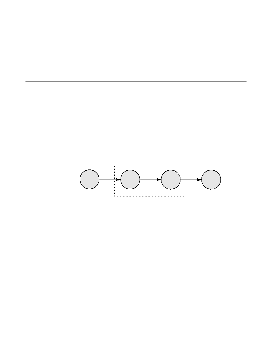
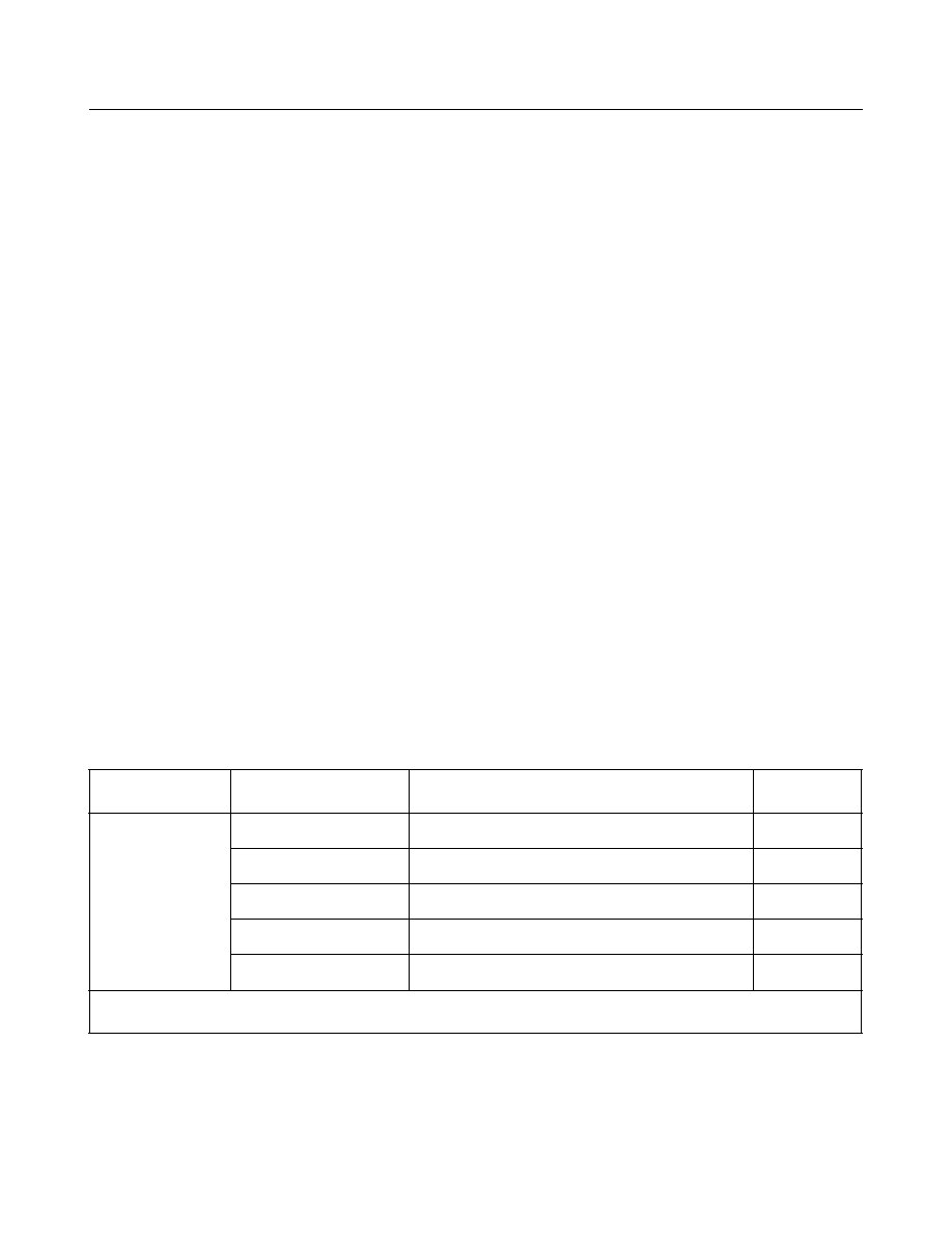
Pipeline Architecture
The LR4102 implements a 3-stage pipeline (Fetch, Execute, and
Writeback) that uses a single adder for the ALU, the data address, and
the instruction address. Sharing a single adder dramatically reduces the
circuitry required to implement the microprocessor, and eliminates
pipeline registers and bypass logic. The LR4102 design does not require
a load delay slot.
Figure 2
shows the microprocessor CPU 3-stage
pipeline.
Figure 2
LR4102 CPU Pipeline with X2 Stall Cycle
The execution of a single LR4102 instruction consists of the following
three pipeline stages:
1.
Instruction Fetch ≠ The LR4102 fetches the instruction (IF), and if
necessary, decompresses a 16-bit instruction into a 32-bit
instruction.
2.
Execute ≠ The LR4102 executes all ALU instructions, resolves
conditional branches, and calculates load and store addresses (X1).
The CPU then transfers load or store data from external memory or
cache and performs move to/from coprocessor operations in a second
execute (stall) cycle (X2), which is only inserted when required.
3.
Writeback ≠ The LR4102 writes the results into the register file (WB).
X1
X2
WB
Execute
Writeback
Instruction Fetch
IF
Stall
TinyRISC LR4102 Microprocessor
5
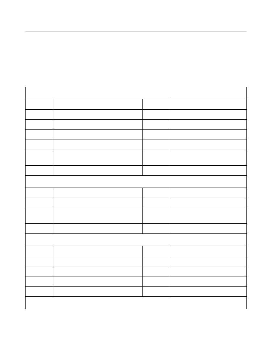
Instruction Set Summary
Table 1
summarizes the 32-bit instruction set for the LR4102, and
Table
2
lists the unimplemented MIPS II instructions.
Table 3
provides a
summary of the LR4102 MIPS16 instruction set.
Table 1
LR4102 32-Bit Instruction Set Summary
Load and Store Instructions
LB
Load Byte
SB
Store Byte
LBU
Load Byte Unsigned
SH
Store Halfword
LH
Load Halfword
SW
Store Word
LHU
Load Halfword Unsigned
SWL
Store Word Left
LW
Load Word
SWR
Store Word Right
LWL
Load Word Left
SYNC
Synchronize (load/store
synchronization)
LWR
Load Word Right
≠
≠
Arithmetic Instructions: ALU Immediate
ADDI
Add Immediate
ORI
OR Immediate
ADDIU
Add Immediate Unsigned
SLTI
Set on Less Than Immediate
ANDI
AND Immediate
SLTIU
Set on Less Than Immediate
Unsigned
LUI
Load Upper Immediate
XORI
Exclusive OR Immediate
Arithmetic Instructions: Three-Operand, Register-Type
ADD
Add
SLT
Set on Less Than
ADDU
Add Unsigned
SLTU
Set on Less Than Unsigned
AND
Logical AND
SUB
Subtract
NOR
Logical NOR
SUBU
Subtract Unsigned
OR
Logical OR
XOR
Logical Exclusive OR
(Sheet 1 of 4)

6
TinyRISC LR4102 Microprocessor
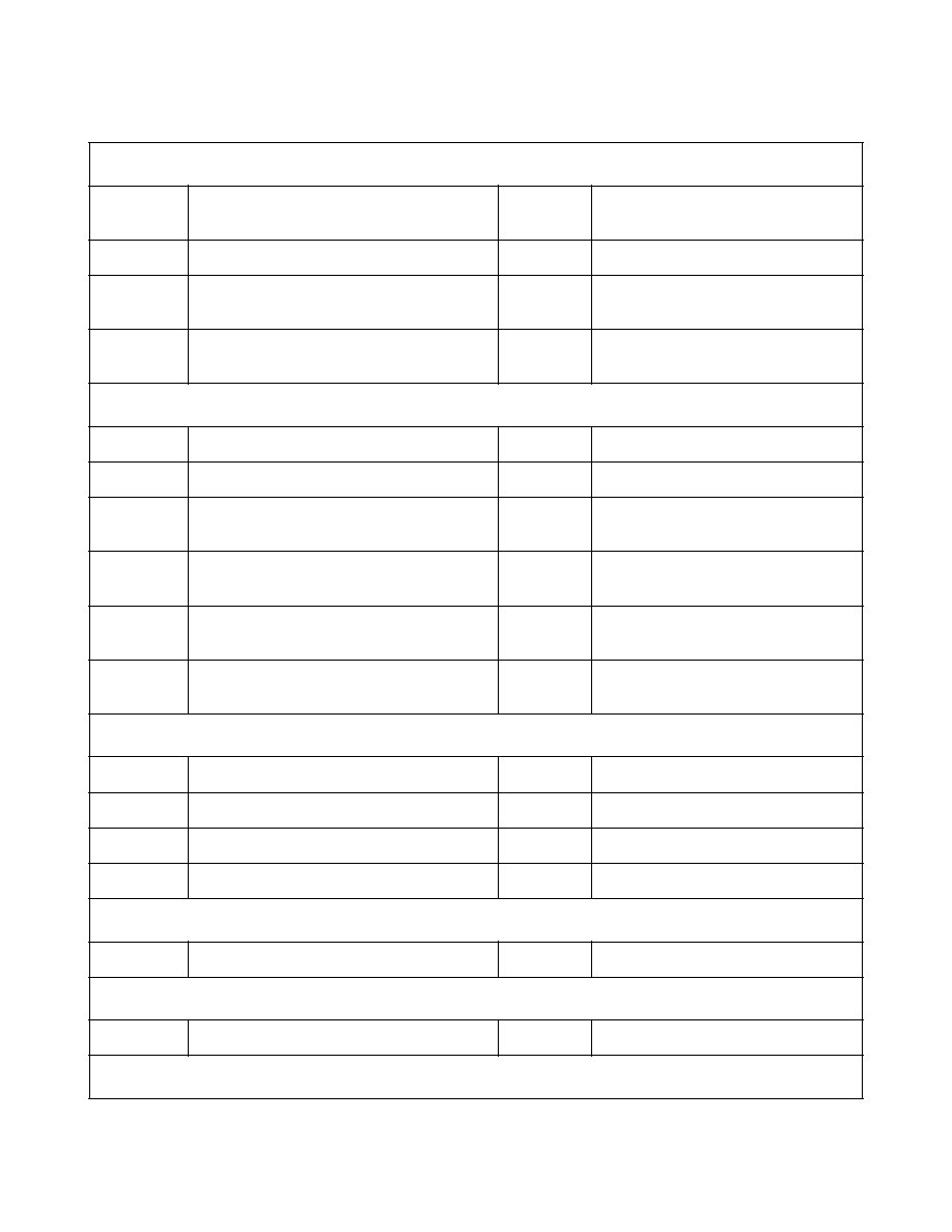
Shift Instructions
SLL
Shift Left Logical
SRAV
Shift Right Arithmetic Variable
SLLV
Shift Left Logical Variable
SRL
Shift Right Logical
SRA
Shift Right Arithmetic
SRLV
Shift Right Logical Variable
Multiply/Divide Instructions
DIV
Divide
MSUBU
1
Multiply Subtract Unsigned
DIVU
Divide Unsigned
MTHI
Move To HI
MADD
1
Multiply Add
MTLO
Move To LO
MADDU
1
Multiply Add Unsigned
MUL
1
Three-Operand Multiply
MFHI
Move From HI
MULT
Multiply
MFLO
Move From LO
MULTU
Multiply Unsigned
MSUB
1
Multiply Subtract
≠
≠
Jump and Branch Instructions
BCzF
Branch on Coprocessor z False
BLTZAL
Branch on Less Than Zero and
Link
BCzT
Branch on Coprocessor z True
BNE
Branch on Not Equal
BEQ
Branch on Equal
J
Jump
BGEZ
Branch on Greater Than or Equal to
Zero
JAL
Jump and Link
BGEZAL
Branch on Greater Than or Equal to
Zero and Link
JALR
Jump and Link Register
BGTZ
Branch on Greater Than Zero
JALX
Jump and Link Exchange
BLEZ
Branch on Less Than or Equal to Zero JR
Jump Register
BLTZ
Branch on Less Than Zero
BGTZL
Branch on Greater Than Zero
Likely
BCzFL
Branch on Coprocessor z False Likely
BLEZL
Branch on Less Than or Equal to
Zero Likely
Table 1
LR4102 32-Bit Instruction Set Summary (Cont.)
(Sheet 2 of 4)
TinyRISC LR4102 Microprocessor
7
Jump and Branch Instructions (Cont.)
BCzTL
Branch on Coprocessor z True Likely
BLTZALL
Branch on Less Than Zero and
Link Likely
BEQL
Branch on Equal Likely
BLTZL
Branch on Less Than Zero Likely
BGEZALL
Branch on Greater Than or Equal to
Zero and Link Likely
BNEL
Branch on Not Equal Likely
BGEZL
Branch on Greater Than or Equal to
Zero Likely
≠
≠
Coprocessor Instructions
BCzF
Branch on Coprocessor z False
MTCz
Move to Coprocessor z
BCzT
Branch on Coprocessor z True
MFCz
Move from Coprocessor z
COPz
Coprocessor Operation
SWCz
Store Word from Coprocessor z
(z
0)
CTCz
Move Control to Coprocessor z
BCzFL
Branch on Coprocessor z False
Likely
CFCz
Move Control from Coprocessor z
BCzTL
Branch on Coprocessor z True
Likely
LWCz
Load Word to Coprocessor z
(z
0)
≠
≠
System Control Coprocessor (CP0)
MFC0
Move from CP0
RFE
Restore from Exception
MTC0
Move to CP0
WAITI
1
Wait for Interrupt
TLBR
Read Indexed TLB Entry
TLBWI
Write Indexed TLB Entry
TLBWR
Write Random TLB Entry
TLBP
Probe TLB for Matching Entry
Special Control Instructions
BREAK
Breakpoint
SYSCALL
System Call
Trap Instructions
TEQ
Trap if Equal
TLT
Trap if Less Than
Table 1
LR4102 32-Bit Instruction Set Summary (Cont.)
(Sheet 3 of 4)

8
TinyRISC LR4102 Microprocessor
Trap Instructions (Cont.)
TEQI
Trap if Equal Immediate
TLTI
Trap if Less Than Immediate
TGE
Trap if Greater Than or Equal
TLTIU
Trap if Less Than Immediate
Unsigned
TGEI
Trap if Greater Than or Equal
Immediate
TLTU
Trap if Less Than Unsigned
TGEIU
Trap if Greater Than or Equal
Immediate Unsigned
TNE
Trap if Not Equal
TGEU
Trap if Greater Than or Equal Unsigned TNEI
Trap If Not Equal Immediate
EJTAG Debug Instructions
SDBBP
Software Debug Breakpoint
DERET
Debug Exception Return
1. LR4102/EZ4102-specific instruction.
Table 2
Unimplemented Instructions Summary
Unimplemented MIPS II Instructions
COP1
All floating-point instructions
ERET
Exception Return
LL
Load Linked Word
LDCz
Load Doubleword to Coprocessor
SC
Store Conditional Word
SDCz
Store Doubleword to Coprocessor
Table 1
LR4102 32-Bit Instruction Set Summary (Cont.)
(Sheet 4 of 4)

TinyRISC LR4102 Microprocessor
9
Table 3
LR4102 16-Bit Instruction Set Summary
Load and Store Instructions
LB
1
Load Byte
LW
1
Load Word
LBU
1
Load Byte Unsigned
SB
1
Store Byte
LH
1
Load Halfword
SH
1
Store Halfword
LHU
1
Load Halfword Unsigned
SW
1
Store Word
Arithmetic Instructions: ALU Immediate
LI
1
Load Immediate
SLTIU
1
Set on Less Than Immediate
Unsigned
ADDIU
1
Add Immediate Unsigned
CMPI
1
Compare Immediate
SLTI
1
Set on Less Than Immediate
≠
≠
Arithmetic Instructions: Two/Three Operand, Register Type
ADDU
Add Unsigned
AND
Logical AND
SUBU
Subtract Unsigned
OR
Logical OR
SLT
Set on Less Than
XOR
Exclusive Logical OR
SLTU
Set on Less Than Unsigned
NOT
Logical NOT
CMP
Compare
MOVE
Move
NEG
Negate
≠
≠
Shift Instructions
SLL
1
Shift Left Logical
SLLV
Shift Left Logical Variable
SRL
1
Shift Right Logical
SRLV
Shift Right Logical Variable
SRA
1
Shift Right Arithmetic
SRAV
Shift Right Arithmetic Variable
(Sheet 1 of 2)

10
TinyRISC LR4102 Microprocessor
Multiply/Divide Instructions
MULT
Multiply
DIVU
Divide Unsigned
MULTU
Multiply Unsigned
MFHI
Move From HI
DIV
Divide
MFLO
Move From LO
Jump and Branch Instructions
JAL
Jump and Link
BNEZ
1
Branch on Not Equal to Zero
JALX
Jump and Link Exchange
BTEQZ
1
Branch on T Equal to Zero
JR
Jump Register
BTNEZ
1
Branch on T Not Equal to Zero
JALR
Jump and Link Register
B
1
Branch Unconditional
BEQZ
1
Branch on Equal to Zero
≠
≠
Special Instructions
EXTEND
Extend
BREAK
Breakpoint
EJTAG Debug Instructions
SDBBP
Software Debug Breakpoint
≠
≠
1. Extensible instruction; for details, please see the documentation on the MIPS16 Application Specific
Extension to the MIPS ISA, which is available from MIPS Technologies Incorporated.
Table 3
LR4102 16-Bit Instruction Set Summary (Cont.)
(Sheet 2 of 2)
TinyRISC LR4102 Microprocessor
11
LR4102 Register Map
Table 4
shows the LR4102 microprocessor register memory map.
Table 4
LR4102 Register Memory Map
Register Name
Physical Address
Description
System configuration registers in BBCC
SCR1
0x1FFF.0000
System Configuration Register 1
SCR2
0x1FFF.0004
System Configuration Register 2
SCR3
0x1FFF.0008
System Configuration Register 3
Timer registers
T0ICR
0x1FFF.0100
Timer 0 Initial Count Register
T0CCR
0x1FFF.0104
Timer 0 Current Count Register
T1ICR
0x1FFF.0108
Timer 1 Initial Count Register
T1CCR
0x1FFF.010C
Timer 1 Current Count Register
TMR
0x1FFF.0110
Mode Register
TISR
0x1FFF.0114
Interrupt Status Register
SerialICE-1 Port (UART) registers
RxStatus
0x1FFF.0200
Receive (Rx) Status Register (Reading)
RxSetup
0x1FFF.0200
Receive (Rx) Setup Register (Writing)
RxData
0x1FFF.0204
Receive (Rx) Data Register
TxStatus
0x1FFF.0208
Transmit (Tx) Status Register
TxData
0x1FFF.020C
Transmit (Tx) Data Register
Reserved registers
Reserved
0x1FFF.0300≠.03FF
Reserved for LSI Logic use
FBus registers
FACFG0
0x1FFF.0400
Configuration for address range 0
FACFG1
0x1FFF.0404
Configuration for address range 1
(Sheet 1 of 2)

12
TinyRISC LR4102 Microprocessor
FBus registers (Cont.)
FACFG2
0x1FFF.0408
Configuration for address range 2
FACFG3
0x1FFF.040C
Configuration for address range 3
FACFG4
0x1FFF.0410
Configuration for address range 4
FACFG5
0x1FFF.0414
Configuration for address range 5
FBUSTA
0x1FFF.0418
Bus turnaround register for address range 0≠5
FACMP0
0x1FFF.0440
Address compare register address range 0
FACMP1
0x1FFF.0444
Address compare register address range 1
FACMP2
0x1FFF.0448
Address compare register address range 2
FACMP3
0x1FFF.044C
Address compare register address range 3
FACMP4
0x1FFF.0450
Address compare register address range 4
FACMP5
0x1FFF.0454
Address compare register address range 5
FBUSCMP
0x1FFF.0470
Address compare register for FBus address range.
FBUSAC
0x1FFF.0474
Address compare register for FBus I/O, memory, and
configuration address range.
FBUSCFG
0x1FFF.0480
Configuration for FBus when accessing outside
programmable address range 0≠5.
FSDRAM
0x1FFF.0490
Configuration for external EDO (S)DRAM
FDRAMT
0x1FFF.0494
Timing parameters for external EDO DRAM
FSDRAMT
0x1FFF.0498
Timing parameters for external SDRAM
FGPCFG
0x1FFF.04C0
Configuration for General-Purpose I/O
FGPOUTPUT
0x1FFF.04C4
Output value for General-Purpose Outputs
FGPINPUT
0x1FFF.04C8
Input value for General-Purpose Inputs
Reserved registers
Reserved
0x1FFF.0500≠.06FF
Reserved for LSI Logic use
On Chip Memory (OCM), 1 Kbytes
OCM area
0x1FFF.8000≠.83FF
On chip memory. Placed on CBus, 1 cycle access
Table 4
LR4102 Register Memory Map (Cont.)
Register Name
Physical Address
Description
(Sheet 2 of 2)
TinyRISC LR4102 Microprocessor
13
Signal Descriptions
The signals are described in alphabetical order by mnemonic. Each
signal definition contains the mnemonic and the full signal name.
Mnemonics for signals that are active LOW end in an "N", and
mnemonics for signals that are active HIGH end in a "P." In the
descriptions that follow, the verb
assert means to drive active. The verb
deassert means to drive inactive.
The LR4102 signals are divided into the following groups:
∑
Control Signals
∑
Clocking Interface
∑
Timer Interface
∑
SerialICE-1 Interface
∑
EJTAG Interface and JTAG boundary scan signals
∑
PC Trace Output
∑
FBus Interface
∑
Test Interface
∑
Power Lines
Table 5
lists all of the LR4102 signals, grouped by interface.
Table 5
LR4102 Signal List
Signal Group
Mnemonic Name
Functional Description
I/O
Control Signals
RESETN
Asynchronous system reset
Input
BIG_ENDIANP
Big/Little Endian select
Input
CWAITIP
Wait for interrupt (low power mode)
Output
INTP[5:0]
Condition/Interrupt
Input
DEBUGMP
Debug mode
Output
(Sheet 1 of 4)
14
TinyRISC LR4102 Microprocessor
Clocking
Interface
EXTAL
Input from crystal/Oscillator
Input
XTAL
Output to crystal
Output
PBCLKP
FAPI clock
Output
SDCLKP
SDRAM clock
Output
DIVC[1:0]
The divide value for DIV C upon reset
Input
DIVA[1:0]
The divide value for DIV A
Input
SELECT_PLLN
Control clock source MUX
Input
RESET_OUTN
Delayed reset signal for FAPI bus
Output
PLLENP
Enable PLL
Input
PLLENARSTP
Enable PLL auto reset
Input
Timer Interface
T0_OUTN
Timer 0 output
Output
T1_OUTN
Timer 1 output
Output
SerialICE-1
Interface
ICECLKP
SerialICE-1 Port clock
Input
ICERXP
SerialICE-1 Port receive
Input
ICETXP
SerialICE-1 Port transmit
Output
EJTAG Interface
and JTAG
boundary scan
signals
TCK
EJTAG Interface clock
Input
TMS
EJTAG Interface mode select
Input
TDI_DINT
EJTAG Interface data in/Debug interrupt
Input
TDO_TPC
EJTAG Interface data out/PC out
Output
TRST
EJTAG Interface reset
Input
PC Trace Output DCLK
PC Trace clock output
Output
PCST1[2:0]
PC Trace status set 1 [2:0]
Output
TPC[4:2]
PC Trace PC out [4:2]
Output
Table 5
LR4102 Signal List (Cont.)
Signal Group
Mnemonic Name
Functional Description
I/O
(Sheet 2 of 4)
TinyRISC LR4102 Microprocessor
15
FBus Interface
CBEN[3:0]
Command/byte enable
Bidirectional
DEVSELN
Device select
Bidirectional
FADDRP[28:0]
Demultiplexed address bus
Output
FADP[31:0]
Multiplexed address/Data bus
Bidirectional
FALEP
Address latch enable
Output
FRAMEN
Cycle frame indicating a bus transaction is
beginning
Bidirectional
GNTN
Grant the FBus
Output
GP[5:0]
General-purpose pins
Bidirectional
GPIO[3:0]
General-purpose I/O pins
Bidirectional
GPRDN
General-purpose read enable
Output
GPWEN[3:0]
General-purpose write byte enable
Output
IRDYN
Initiator ready
Bidirectional
REQN
Request FBus
Input
SD_CASN0_DMP0
DRAM CAS0 or SDRAM data mask 0
Output
SD_CASN1_DMP1
DRAM CAS1 or SDRAM data mask 1
Output
SD_CASN2_DMP2
DRAM CAS2 or SDRAM data mask 2
Output
SD_CASN3_DMP3
DRAM CAS3 or SDRAM data mask 3
Output
SD_OEN_CASN
DRAM output enable or SDRAM CAS
Output
SDONEP
Snooping done
Output
SD_RASN
SDRAM RAS
Output
SD_RASN0_CSN0
DRAM RAS bank 0 or SDRAM CAS0
Output
SD_RASN1_CSN1
DRAM RAS bank 1 or SDRAM CAS1
Output
SD_WEN_WEN
DRAM write enable or SDRAM write enable Output
STOPN
Stop transaction
Bidirectional
Table 5
LR4102 Signal List (Cont.)
Signal Group
Mnemonic Name
Functional Description
I/O
(Sheet 3 of 4)
16
TinyRISC LR4102 Microprocessor
FBus Interface
TRDYN
Target ready
Bidirectional
Test Interface
CSHTSTP
Cache test enable
Input
IDDTN
IDD test
Input
JTAGALSOP
JTAG controller present
Input
PMON_OUTP
Process monitor output
Output
SCAN_ENABLEP
Enable scan chain loading
Input
SCAN__INP
Input to the scan chain
Input
SCAN_MODEP
Enable scan testing
Input
SCAN_OUTP
Output from the scan chain
Output
SCAN_RAMWEP
RAM write enable
Input
SELECT_CKOUT1N
Select PLL test
Input
TN
3-state all LR4102 output and bidirectional
signals
Input
Power Lines
VDD, VDD2
V
DD
for CPU core and oscillator 2.5 V or
1.8 V
Power
VDD4
V
DD
for I/O 3.3 V
Power
PLLVDD1
V
DD
to PLL 2.5 V. Requires V
DD
CPU core
and oscillator at 2.5 V, since PLL must be
disabled for V
DD
CPU core and clock at
1.8 V
Power
VSS, VSS2, VSS4,
PLLVSS1
V
SS
for CPU core, clock, I/O and PLL
Power
Table 5
LR4102 Signal List (Cont.)
Signal Group
Mnemonic Name
Functional Description
I/O
(Sheet 4 of 4)

TinyRISC LR4102 Microprocessor
17
LR4102 Specifications
This section specifies the LR4102 electrical characteristics and includes
the following subsections:
∑
"AC Timing"
∑
"Electrical Requirements"
AC Timing
This section describes the AC timing characteristics of the LR4102
interface. Figures
3
and
4
show the EXTAL and TCK clocks. Figures
5
through
9
illustrate the input and output timing relationship with respect
to various clocks (PBCLKP, SDCLKP, and DCLKP). Tables
6
through
14
list the minimum and maximum input and output values for the LR4102
interface signals. Note that all output signals have a 65 pF load.
Figure 3
EXTAL Clock Timing
Figure 4
TCK Clock Timing
1
EXTAL
2
TCK

18
TinyRISC LR4102 Microprocessor
Figure 5
Input Timing with Respect to PBCLKP
Figure 6
Output Timing with Respect to PBCLKP
Figure 7
Input Timing with Respect to SDCLKP
Setup
Input
PBCLKP
Hold
Note: PBCLKP equals the system clock (PCLKP) when the DIV C value in the Clock
module is 0b01. DIV C = 0b01 is used to show timing for signals related to the system
clock. The setting of DIV C only affects PBCLKP and the timing for signals related to
the FAPI clock (PBCLKP).
Min Output
Output
PBCLKP
Max Output
Setup
Input
SDCLKP
Hold

TinyRISC LR4102 Microprocessor
19
Figure 8
Output Timing with Respect to SDCLKP
Figure 9
Output Timing with Respect to DCLK
Table 6
EXTAL Input Timing
Parameter
Input
Signal
Clock
Period
Frequency
Min
Max
Units
1
EXTAL
5.88 ns
≠
170
MHz
Table 7
TCK Input Timing
Parameter
Input
Signal
Clock
Period
Frequency
Min
Max
Units
2
TCK
11.76 ns
≠
85
MHz
Min Output
Output
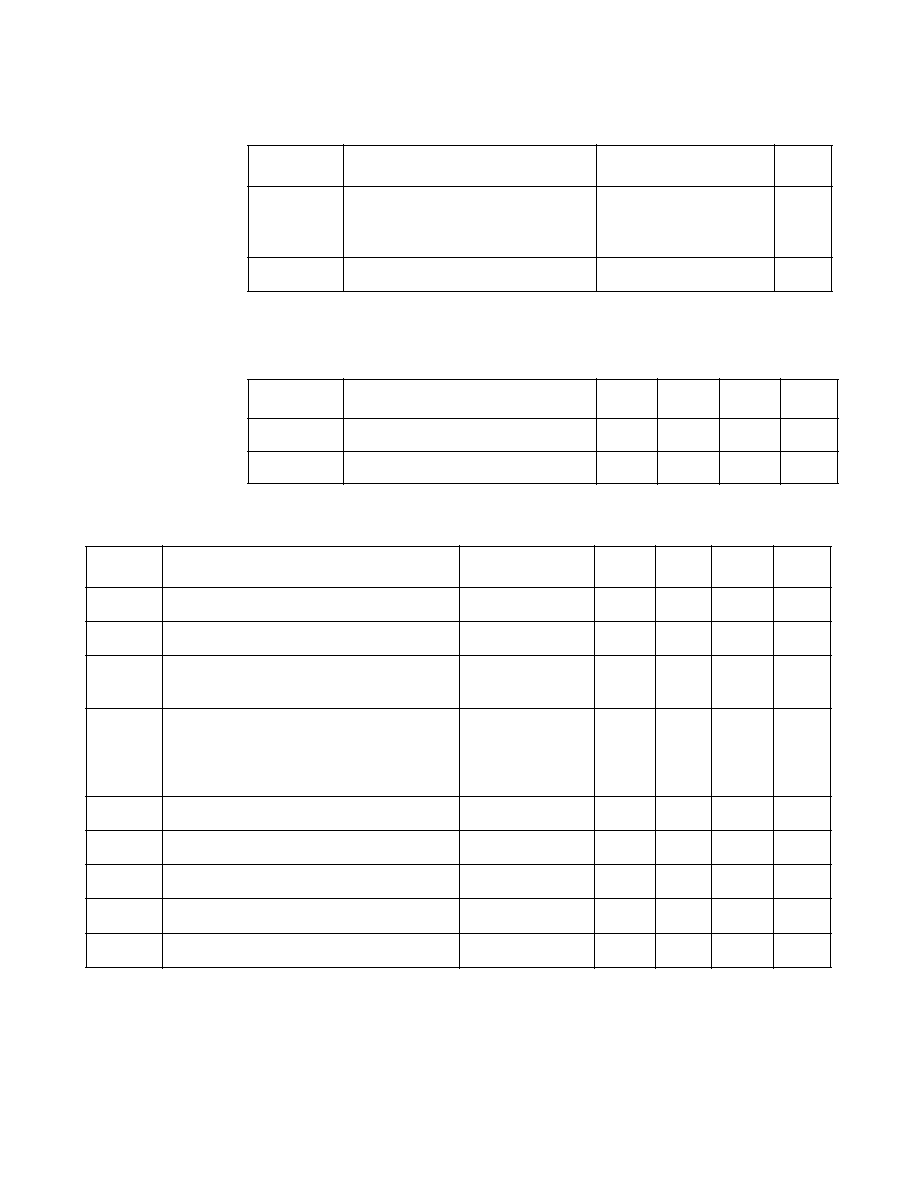
SDCLKP
Max Output
Min Output
Output
DCLK
Max Output
20
TinyRISC LR4102 Microprocessor
Table 8
AC Input Timing with respect to rising edge of PBCLKP
1
1. With 65 pF load
2. This signal is related to the system clock, but not to the FAPI bus (see
Figure 5
note).
3. This signal is related to both the system clock and the FAPI bus (see
Figure 5
note).
Input Signal
Setup
Hold
Units
CBEN[3:0]
7.2
1.4
ns
DEVSELN
4.7
2.2
ns
FADP[31:0]
3
2.9
2.7
ns
FRAMEN
7.4
2.2
ns
GP[5:0]
2
2.8
2.6
ns
GPIO[3:0]
2
1.8
2.8
ns
IRDYN
7.5
1.9
ns
REQN
3.5
1.5
ns
STOPN
4.7
1.7
ns
TRDYN
4.6
2.0
ns
Table 9
AC Input Timing with respect to rising edge of SDCLKP
1
1. With 65 pF load.
Input Signal
Setup
Hold
Units
FADP[31:0]
2.0
3.4
ns
Table 10
AC Input Timing with respect to rising edge of TCK
Input
Setup
Hold
Units
TDI_DINT
1.9
1.1
ns
TMS
1.6
0.7
ns

TinyRISC LR4102 Microprocessor
21
Table 11
AC Output Timing with respect to rising edge of
PBCLKP
1
Output Signal
1
Min
Max
Units
CBEN[3:0]
1.0
8.0
ns
CWAITIP
2
2.8
8.8
ns
DEBUGMP
3.1
9.3
ns
DEVSELN
0.8
7.2
ns
FADDRP[28:0]
2
1.3
6.2
ns
FADP[31:0]
3
0.8
7.4
ns
FALEP
1.6
6.1
ns
FRAMEN
1.0
7.5
ns
GNTN
2.3
7.0
ns
GP[5:0]
2
0.4
7.0
ns
GPIO[3:0]
2
0.3
6.8
ns
GPRDN
2
1.7
5.8
ns
GPWEN[3:0]
2
1.4
6.2
ns
IRDYN
1.0
7.5
ns
RESET_OUTN
2
2.1
7.3
ns
SD_CASN[3:0]_DMP[3:0]
2
1.3
6.0
ns
SD_OEN_CASN
2
1.4
5.9
ns
SDONEP
1.8
6.4
ns
SD_RASN[1:0]_CSN[1:0]
2
1.3
5.9
ns
SD_WEN_WEN
2
1.4
5.7
ns
STOPN
0.8
7.2
ns
T0_OUTN
2
2.6
8.8
ns
(Sheet 1 of 2)
22
TinyRISC LR4102 Microprocessor
T1_OUTN
2
2.7
8.9
ns
TRDYN
0.8
7.2
ns
1. With 65 pF load
2. This signal is related to the system clock, but not to the FAPI bus (see
Figure 5
note).
3. This signal is related to both the system clock and the FAPI bus (see
Figure 5
note).
Table 12
AC Output Timing with respect to rising edge of
SDCLKP
1
1. With 65 pF load.
Output Signal
1
Min
Max
Units
FADDRP[28:0]
1.7
6.9
ns
FADP[31:0]
1.2
8.3
ns
SD_CASN[3:0]_DMP[3:0]
1.7
6.9
ns
SD_OEN_CASN
1.8
6.6
ns
SD_RASN
1.7
6.4
ns
SD_RASN[1:0]_CSN[1:0]
1.7
6.8
ns
SD_WEN_WEN
1.8
6.6
ns
Table 13
AC Output Timing with respect to falling edge of TCK
Output Signal
1
1. With 65 pF load
Min
Max
Units
TDO_TPC
2.1
8.9
ns
Table 11
AC Output Timing with respect to rising edge of
PBCLKP
1
(Cont.)
Output Signal
1
Min
Max
Units
(Sheet 2 of 2)
TinyRISC LR4102 Microprocessor
23
Note:
there is no setup/hold time requirements for the interrupt
pins, INTP[5:0], because they are synchronized internally
within the LR4102.
Electrical Requirements
This section contains the electrical parameters for the TinyRISC LR4102
Microprocessor in the following tables:
∑
Table 15
lists the absolute maximum ratings
∑
Table 16
defines the recommended operating supply voltage and
temperature
∑
Table 17
shows the pin capacitance
∑
Table 18
lists the DC characteristics
Table 14
EZ4102 AC Output Timing with respect to rising edge of
DCLK
1
Output Signal
1
1.
With 65 pF load.
Min
Max
Units
PCST1[2:0]
-
2.9
1.9
ns
TDO_TPC
-
3.2
1.8
ns
TPC[4:2]
-
3.2
2.0
ns
Table 15
Absolute Maximum Rating
1
1. Exceeding these values may cause damage to the LR4102.
Symbol
Parameter
Limits
Unit
V
DD/DD2
DC Supply Voltage
2
, core and oscillator
2. Referenced to V
SS
.
-
0.3 to 3.1
V
V
DD4
3.3 V DC Supply Voltage
2
, I/O
-
0.3 to 3.9
V
V
IN
3.3 V Drive Input Voltage
2
-
1.0 to V
DD4
+ 0.3
V
T
STG
Storage Temperature Range (Plastic)
-
40 to 125
∞C
24
TinyRISC LR4102 Microprocessor
Table 16
Recommended Operating Conditions
Symbol
Parameter
Limits
Unit
V
DD/DD2
DC Supply Voltage
1
at V
DD
/V
DD2
nominal 1.8 V
at V
DD
/V
DD2
nominal 2.5 V
1. Referenced to V
SS
.
1.71 to 1.89
2.38 to 2.63
V
V
T
A
Ambient Temperature
0 to 70
∞C
Table 17
Capacitance
Symbol
Parameter
Min
Typ
Max
Unit
C
IN
Input Capacitance
4.6
≠
5.2
pF
C
OUT
Output Capacitance
4.6
≠
5.2
pF
Table 18
DC Characteristics
Symbol
Parameter
Condition
1
1. Specified at V
DD4
equals 3.3 V
±
5% at ambient temperature over the specified range.
Min
Typ
Max
Units
V
DD4
Supply Voltage, I/O
≠
3.0
3.3
3.6
V
V
IL
Voltage Input Low
≠
-
0.5
≠
0.8
V
V
IH
Voltage Input High
≠
2.0
≠
V
DD4
+ 0.3
V
I
IL
Current Input Leakage
Inputs with no Pull-up/-down Resistor
Inputs with Pull-down Resistor
Inputs with Pull-up Resistor
V
IN
= V
SS
/V
DD4
V
IN
= V
DD4
V
IN
= V
SS
-
10
35
-
35
±
1
115
-
115
10
222
-
214
µ
A
µ
A
µ
A
V
OL
Voltage Output Low
≠
≠
0.2
0.4
V
V
OH
Voltage Output High
≠
2.4
≠
V
DD4
V
I
DD
Quiescent Supply Current
≠
<1
20
100
µ
A
I
CC
Dynamic Supply Current
≠
≠
170
≠
mA
I
OZ
Z-state Output Leakage Current
V
OH
= V
SS
/V
DD4
-
10
±
1
10
µ
A

TinyRISC LR4102 Microprocessor
25
Pinouts
Table 19
provides an alphabetical pinout list for the LR4102 256-pin
PBGA.
Table 19
LR4102 256-pin PBGA Pinout
BIG_ENDIANP
E18
CBEN0
A20
CBEN1
F18
CBEN2
Y9
CBEN3
W5
CWAITIP1
D10
CSHTSTP
B18
DCLK
T1
DEBUGMP
P4
DEVSELN
Y11
DIVA0
G17
DIVA1
K17
DIVC0
K18
DIVC1
L18
EXTAL
B16
FADDRP0
K20
FADDRP1
K19
FADDRP2
L20
FADDRP3
L19
FADDRP4
M20
FADDRP5
M19
FADDRP6
N20
FADDRP7
N19
FADDRP8
P20
FADDRP9
P19
FADDRP10
R20
FADDRP11
R19
FADDRP12
T20
FADDRP13
T19
FADDRP14
U20
FADDRP15
U19
FADDRP16
V20
FADDRP17
V19
FADDRP18
W20
FADDRP19
Y20
FADDRP20
W19
FADDRP21
Y19
FADDRP22
V18
FADDRP23
Y18
FADDRP24
W18
FADDRP25
Y17
FADDRP26
W17
FADDRP27
Y16
FADDRP28
W16
FADP0
B19
FADP1
B20
FADP2
C19
FADP3
C20
FADP4
D19
FADP5
D20
FADP6
E19
FADP7
E20
FADP8
F20
FADP9
F19
FADP10
G20
FADP11
G19
FADP12
H20
FADP13
H19
FADP14
J20
FADP15
J19
FADP16
W9
FADP17
Y8
FADP18
W8
FADP19
Y7
FADP20
W7
FADP21
Y6
FADP22
W6
FADP23
Y5
FADP24
Y4
FADP25
W4
FADP26
Y3
FADP27
W3
FADP28
Y2
FADP29
W2
FADP30
Y1
FADP31
W1
FALEP
Y13
FRAMEN
W10
GNTN
V2
GP0
V15
GP1
U14
GP2
V14
GP3
V13
GP4
U7
GP5
V6
GPIO0
T18
GPIO1
V16
GPIO2
V5
GPIO3
V3
GPRDN
U9
GPWEN0
V10
GPWEN1
V9
GPWEN2
V8
GPWEN3
V7
ICECLKP
A8
ICERXP
B9
ICETXP
A9
IDDTN
D12
INTP0
A13
INTP1
B13
INTP2
C13
INTP3
A12
INTP4
A11
INTP5
A10
IRDYN
Y10
JTAGALSOP
C9
PBCLKP
Y12
PCST10
T3
PCST11
R3
PCST12
P3
PLLENARSTP
G18
PLLENP
H18
PLLVDD1
A17
PLLVSS1
A18
PMON_OUTP
B11
REQN
V1
RESET_OUTN
A14
RESETN
A15
SCAN_ENABLEP
C17
SCAN_INP
J18
SCAN_MODEP
C14
SCAN_OUTP
B17
SCAN_RAMWEP
D16
SD_CASN0_DMP0
N18
SD_CASN1_DMP1
P17
SD_CASN2_DMP2
Y14
SD_CASN3_DMP3
W14
SD_OEN_CASN
M18
SD_RASN
R18
SD_RASN0_CSN0
P18
SD_RASN1_CSN1
W15
SD_WEN_WEN
M17
SDCLKP
Y15
SDONEP
W13
SELECT_CKOUT1N
B14
SELECT_PLLN
B15
STOPN
W12
T0_OUTN
C10
T1_OUTN
B10
TCK
U1
TDI_DINT
T2
TDO_TPC
R2
TMS
U2
TN
C11
TPC2
R1
TPC3
P2
TPC4
P1
TRDYN
W11
TRST
N3
VDD
D14
VDD2
L3
VDD2
L4
VDD2
T4
VDD2
U3
VDD2
V11
VDD2
U11
VDD2
U16
VDD2
V17
VDD2
J 17
VDD2
E17
VDD2
D18
VDD2
D5
VDD2
C4
VDD4
D6
VDD4
D11
VDD4
D15
VDD4
F4
VDD4
F17
VDD4
K4
VDD4
L17
VDD4
R4
VDD4
R17
VDD4
U6
VDD4
U10
VDD4
U15
VSS
A1
VSS
C15
VSS
C16
VSS2
D3
VSS2
E4
VSS2
M3
VSS2
M4
VSS2
V4
VSS2
U5
VSS2
V12
VSS2
U12
VSS2
U18
VSS2
T17
VSS2
C18
VSS2
A19
VSS2
D9
VSS4
D4
VSS4
D8
VSS4
D13
VSS4
D17
VSS4
H4
VSS4
H17
VSS4
N4
VSS4
N17
VSS4
U4
VSS4
U8
VSS4
U13
VSS4
U17
XTAL
A16
Signal
Solder
Name
Ball
Signal
Solder
Name
Ball
Signal
Solder
Name
Ball
Signal
Solder
Name
Ball
26
TinyRISC LR4102 Microprocessor
Input/Output Drivers
Table 20
lists the I/O driver types.
Table 20
I/O Driver Types
Signal Name
I/O Driver Type Description
BIG_ENDIANP
IBUFULS
Input buffer with pull-up
CBEN[3:0]
BD12CLS
12 mA Bi-directional buffer
CSHTSTP
IBUFULS
Input buffer with pull-up
CWAITIP
BT8LS
8 mA output buffer
DCLK
BT24LS
24 mA output buffer
DEBUGMP
BT8LS
8 mA output buffer
DEVSELN
BD12CULS
12 mA Bi-directional buffer with pull-up
DIVA[1:0]
IBUFLS
Input buffer
DIVC[1:0]
IBUFLS
Input buffer
EXTAL, XTAL
OSCIM
Oscillator
FADDRP[28:0]
BT12LS
12 mA output buffer
FADP[31:0]
BD12CLS
12 mA Bi-directional buffer
FALEP
BT12LS
12 mA output buffer
FRAMEN
BD12CULS
12 mA Bi-directional buffer with pull-up
GNTN
BT12LS
12 mA output buffer
GP[5:0]
BD12SCUHO
12 mA Bi-directional buffer with
Schmidt trigger input and pull-up
GPIO[3:0]
BD12SCUHO
12 mA Bi-directional buffer with
Schmidt trigger input and pull-up
GPRDN
BT12LS
12 mA output buffer
GPWEN[3:0]
BT12LS
12 mA output buffer
ICECLKP
SCHMITCUHO
Schmidt trigger input with pull-up
(Sheet 1 of 3)

TinyRISC LR4102 Microprocessor
27
ICERXP
SCHMITCUHO
Schmidt trigger input with pull-up
ICETXP
BT6LS
6 mA output buffer
IDDTN
IIDDTNLS
IDD test input buffer
INTP[5:0]
IBUFULS
Input buffer with pull-up
IRDYN
BD12CULS
12 mA Bi-directional buffer with pull-up
JTAGALSOP
IBUFULS
Input buffer with pull-up
PBCLKP
BT8LS
8 mA output buffer
PCST[12:10]
BD8CDLS
8 mA Bi-directional buffer with pull-
down
PLLENARSTP
IBUFLS
Input buffer
PLLENP
IBUFLS
Input buffer
PLLVDD1
PLLVDD
PLL Vdd
PLLVSS1
PLLVSS
PLL Vss
PMON_OUTP
PROCMONLS
PROCMON test output driver
REQN
IBUFULS
Input buffer with pull-up
RESET_OUTN
BT8LS
8 mA output buffer
RESETN
IBUFULS
Input buffer with pull-up
SCAN_ENABLEP
IBUFLS
Input buffer
SCAN_INP
IBUFLS
Input buffer
SCAN_MODEP
IBUFDLS
Input buffer with pull-down
SCAN_OUTP
BT8LS
8 mA output buffer
SCAN_RAMWEP
SCHMITCHO
Schmidt trigger input buffer
SD_CASN0_DMP0
BT12LS
12 mA output buffer
SD_CASN1_DMP1
BT12LS
12 mA output buffer
SD_CASN2_DMP2
BT12LS
12 mA output buffer
SD_CASN3_DMP3
BT12LS
12 mA output buffer
Table 20
I/O Driver Types (Cont.)
(Sheet 2 of 3)

28
TinyRISC LR4102 Microprocessor
SD_OEN_CASN
BT12LS
12 mA output buffer
SD_RASN
BT12LS
12 mA output buffer
SD_RASN0_CSN0
BT12LS
12 mA output buffer
SD_RASN1_CSN1
BT12LS
12 mA output buffer
SD_WEN_WEN
BT12LS
12 mA output buffer
SDCLKP
BT8LS
8 mA output buffer
SDONEP
BT12LS
12 mA output buffer
SELECT_CKOUT1N
IBUFLS
Input buffer
SELECT_PLLN
IBUFLS
Input buffer
STOPN
BD12CULS
12 mA Bi-directional buffer with pull-up
T0_OUTN
BT8LS
8 mA output buffer
T1_OUTN
BT8LS
8 mA output buffer
TCK
IBUFULS
Input buffer with pull-up
TDI_DINT
IBUFULS
Input buffer with pull-up
TDO_TPC
BT8LS
8 mA output buffer
TMS
IBUFULS
Input buffer with pull-up
TN
IBUFULS
Input buffer with pull-up
TPC[4:2]
BD8CDLS
8 mA Bi-directional buffer with pull-
down
TRDYN
BD12CULS
12 mA Bi-directional buffer with pull-up
TRST
IBUFULS
Input buffer with pull-up
Table 20
I/O Driver Types (Cont.)
(Sheet 3 of 3)
TinyRISC LR4102 Microprocessor
29
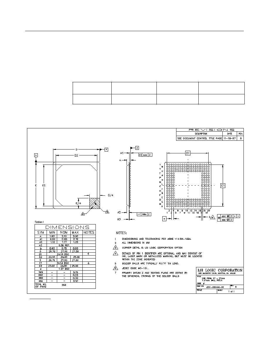
Package and Ordering Information
The LR4102 is available in a 256-lead Plastic Ball Grid Array (PBGA).
Table 21
provides the LR4102 order number and
Figure 10
contains the
package mechanical drawing.
Figure 10
LR4102 256 PBGA (IF) Mechanical Drawing
Table 21
LR4102 Ordering Information
Order Number
Clock Frequency
Package Type
Operating Range
L9A0212
1
1. Order number subject to change
85 MHz
256-lead PBGA
Commercial
MD98.IF
Important:
This drawing may not be the latest version. For board layout and manufacturing, obtain the
most recent engineering drawings from your LSI Logic marketing representative by
requesting the outline drawing for package code IF.

30
TinyRISC LR4102 Microprocessor
Notes

TinyRISC LR4102 Microprocessor
31
Notes

To receive product literature, visit us at http://www.lsilogic.com
LSI Logic Corporation reserves the right to make changes
to any products and services herein at any time without
notice. LSI Logic does not assume any responsibility or lia-
bility arising out of the application or use of any product or
service described herein, except as expressly agreed to in
writing by LSI Logic; nor does the purchase, lease, or use
of a product or service from LSI Logic convey a license
under any patent rights, copyrights, trademark rights, or any
other of the intellectual property rights of LSI Logic or of
third parties.
This document is preliminary. As such, it contains data
derived from functional simulations and performance esti-
mates. LSI Logic has not verified the functional descriptions
or electrical and mechanical specifications using production
parts.
The LSI Logic logo design, CoreWare, G11, TinyRISC and
SerialIce are registered trademarks or trademarks of
LSI Logic Corporation. All other brand and product names
may be trademarks of their respective companies.
BM
Printed in USA
Order No. C14063.A
Doc. No. DB08-000082-01
Printed on
Recycled Paper
ISO 9000 Certified
Sales Offices and Design Resource Centers
LSI Logic Corporation
Corporate Headquarters
Tel: 408.433.8000
Fax: 408.433.8989
NORTH AMERICA
California
Irvine
Tel: 949.809.4600
Fax: 949.809.4444
Pleasanton Design Center
Tel: 925.730.8800
Fax: 925.730.8700
San Diego
Tel: 858.467.6981
Fax: 858.496.0548
Silicon Valley
Tel: 408.433.8000
Fax: 408.954.3353
Wireless Design Center
Tel: 858.350.5560
Fax: 858.350.0171
Colorado
Boulder
Tel: 303.447.3800
Fax: 303.541.0641
Colorado Springs
Tel: 719.533.7000
Fax: 719.533.7020
Fort Collins
Tel: 970.223.5100
Fax: 970.206.5549
Florida
Boca Raton
Tel: 561.989.3236
Fax: 561.989.3237
Georgia
Alpharetta
Tel: 770.753.6146
Fax: 770.753.6147
Illinois
Oakbrook Terrace
Tel: 630.954.2234
Fax: 630.954.2235
Kentucky
Bowling Green
Tel: 270.793.0010
Fax: 270.793.0040
Maryland
Bethesda
Tel: 301.897.5800
Fax: 301.897.8389
Massachusetts
Waltham
Tel: 781.890.0180
Fax: 781.890.6158
Burlington - Mint Technology
Tel: 781.685.3800
Fax: 781.685.3801
Minnesota
Minneapolis
Tel: 612.921.8300
Fax: 612.921.8399
New Jersey
Red Bank
Tel: 732.933.2656
Fax: 732.933.2643
Cherry Hill - Mint Technology
Tel: 856.489.5530
Fax: 856.489.5531
New York
Fairport
Tel: 716.218.0020
Fax: 716.218.9010
North Carolina
Raleigh
Tel: 919.785.4520
Fax: 919.783.8909
Oregon
Beaverton
Tel: 503.645.0589
Fax: 503.645.6612
Texas
Austin
Tel: 512.388.7294
Fax: 512.388.4171
Plano
Tel: 972.244.5000
Fax: 972.244.5001
Houston
Tel: 281.379.7800
Fax: 281.379.7818
Canada
Ontario
Ottawa
Tel: 613.592.1263
Fax: 613.592.3253
INTERNATIONAL
France
Paris
LSI Logic S.A.
Immeuble Europa
Tel: 33.1.34.63.13.13
Fax: 33.1.34.63.13.19
Germany
Munich
LSI Logic GmbH
Tel: 49.89.4.58.33.0
Fax: 49.89.4.58.33.108
Stuttgart
Tel: 49.711.13.96.90
Fax: 49.711.86.61.428
Italy
Milan
LSI Logic S.P.A.
Tel: 39.039.687371
Fax: 39.039.6057867
Japan
Tokyo
LSI Logic K.K.
Tel: 81.3.5463.7821
Fax: 81.3.5463.7820
Osaka
Tel: 81.6.947.5281
Fax: 81.6.947.5287
Korea
Seoul
LSI Logic Corporation of
Korea Ltd
Tel: 82.2.528.3400
Fax: 82.2.528.2250
The Netherlands
Eindhoven
LSI Logic Europe Ltd
Tel: 31.40.265.3580
Fax: 31.40.296.2109
Singapore
Singapore
LSI Logic Pte Ltd
Tel: 65.334.9061
Fax: 65.334.4749
Sweden
Stockholm
LSI Logic AB
Tel: 46.8.444.15.00
Fax: 46.8.750.66.47
Taiwan
Taipei
LSI Logic Asia, Inc.
Taiwan Branch
Tel: 886.2.2718.7828
Fax: 886.2.2718.8869
United Kingdom
Bracknell
LSI Logic Europe Ltd
Tel: 44.1344.426544
Fax: 44.1344.481039
Sales Offices with
Design Resource Centers