 | –≠–ª–µ–∫—Ç—Ä–æ–Ω–Ω—ã–π –∫–æ–º–ø–æ–Ω–µ–Ω—Ç: LS7561 | –°–∫–∞—á–∞—Ç—å:  PDF PDF  ZIP ZIP |
BRUSHLESS DC MOTOR CONTROLLER
FEATURES
∑ Open loop motor control
∑ Tachometer output for closed loop motor control
∑ Error Amplifier and PWM Speed Comparator with full accessibility
∑ High noise immunity Schmitt Triggers on Sensor inputs
∑ 5.5V Reference Supply for external sensors
∑ Cycle-by-cycle current sensing
∑ Static, or current limited dynamic, motor braking
∑ Output enable delay on speed direction reversal
∑ Enable input with fault sensing capability
∑ Fault Indicator output
∑ 60∞/300∞ or 120∞/240∞ electrical sensor spacing selection
∑ Selectable PWM of top and bottom drivers or bottom drivers only
∑ CMOS compatible motor outputs with drive capability
∑ Selectable top driver polarity
∑ Low power dissipation
∑ +10V to +18V Power Supply (V
DD
-Vss)
∑ 28 Pin Plastic DIP (300 mil, 600 mil), 28 Pin SOIC
GENERAL DESCRIPTION
The LS7560/LS7561 are CMOS integrated circuits designed to
control three or four phase brushless DC motors in a closed or
open loop configuration. The IC consists of a decoder which
provides proper commutation sequencing, a frequency-to-
pulse width converter and error amplifier for closed loop motor
speed control, a PWM comparator and sawtooth oscillator for
external driver power control and a 5.5V reference generator
for supplying power to motor sensors. Also included is Fault
detection and indication, overcurrent sensing, dynamic motor
braking, forward/reverse input, sensor spacing selections and
an enable input control. The overcurrent sense condition will
disable all output drivers when using the LS7560 and only the
bottom drivers when using the LS7561.
The IC operates from 10V to 18V and provides CMOS com-
patible outputs for interfacing with external power devices.
Operating below 10V will activate a Fault Indication Output
and disable all Output Drivers.
INPUT/OUTPUT DESCRIPTION: (See Figure 2)
SEQUENCE SELECT Input (Pin 1 )
A High on this input selects 60∞/300∞ and a Low selects 120∞/
240∞ electrical sensor separation. Use of a 300∞ or 240∞ motor
will cause opposite direction rotation as compared to a 60∞ or
120∞ motor.
F/R Input (Pin 27)
A High on this input selects Forward direction and a Low se-
lects Reverse direction. The motor drive outputs are disabled
for 2 clock cycles at the onset of a direction change.
March 1999
1
2
3
4
5
6
7
8
9
10
11
12
13
14
15
16
17
18
19
20
21
22
23
24
25
26
27
28
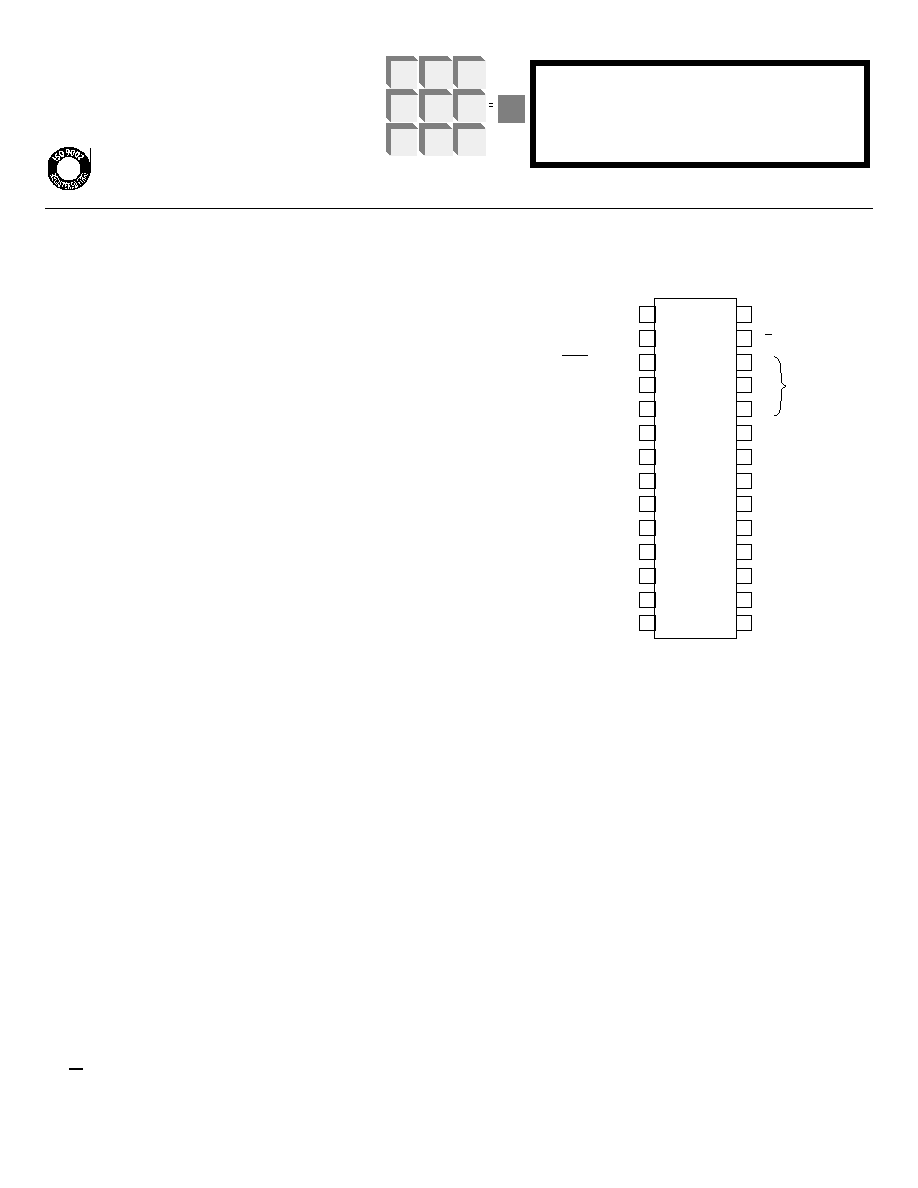
FIGURE 1. PIN CONNECTION DIAGRAM
LS7560
S E Q U E N C E S E L E C T
E N A B L E
FAULT INDICATOR
RC
TACHOMETER OUT
ERROR AMP (+)
ERROR AMP (-)
OSCILLATOR
ERROR AMP OUT
CURRENT SENSE (+)
CURRENT SENSE (-)
OUT 6
OUT 5
OUT 4
OUT 3
OUT 2
OUT 1
V
SS
(-V)
V
R
TOP DRIVER POLARITY SELECT
PWM CONTROL
B R A K E S E L E C T
BRAKE
S1
S2
S3
F/R
V
DD
(+V)
HALL
S E N S O R S
TOP VIEW
S1, S2, S3 Inputs (Pins 24, 25, 26)
Hall Sensor inputs which are decoded to determine the Motor
Commutation Sequence. An invalid input code disables all motor
outputs. Inputs have Schmitt Trigger buffers for noise immunity.
BRAKE Input (Pin 23)
With the BRAKE SELECT input Low, a High on the BRAKE input
forces the Top Drivers to an OFF condition and the Bottom Drivers
to a PWM ON condition. If the Motor is under Closed Loop control,
the Loop is automatically opened and the error amplifier output is
connected to the Error Amp (-) input. By controlling the voltage at
teh Error Amp (+) input, the PWM duty cycle is controlled during
braking. This manner of braking prevents the Bottom Motor Drivers
from drawing excessive current, a condition which can occur during
normal braking, when the Bottom Drivers are turned ON un-
conditionally. With the BRAKE SELECT input High, a High on the
BRAKE input unconditionally causes the Top Drivers to turn OFF
and the Bottom Drivers to turn ON. The BRAKE function has prior-
ity over all other functions.
BRAKE SELECT Input (Pin 22)
A Low on this input selects PWM control of braking and a High se-
lects unconditional braking.
ENABLE Input (Pin 2)
When the ENABLE input is above V
R
/2, all Output Drivers are en-
abled and when it is below V
R
/2.2, all Output Drivers are disabled.
This input has a nominal hysteresis of .05V
R
, where V
R
is the inter-
nally generated Reference Voltage available on Pin 19. Because
the ENABLE input is level sensitive, it can easily be used to control
operation of the IC based on an Analog Fault Condition.
LSI/CSI
LSI Computer Systems, Inc. 1235 Walt Whitman Road, Melville, NY 11747 (516) 271-0400 FAX (516) 271-0405
LS7560/7561
UL
Æ
A3800

ERROR AMPLIFIER Inputs (Pins 6, 7 ) Output (Pin 8)
For closed loop control, the TACHOMETER Output is applied
through a resistor to the negative input of the Error Amplifier on
Pin 7. A speed control potentiometer is connected to the positive
input of the Error Amplifier on Pin 6. A parallel RC Network is con-
nected between the Output of the Error Amplifier on Pin 8 and Pin
7. The Amplifier, configured this way, enables the variable pulse
width to be converted to a DC voltage which is used to control the
motor speed. The potentiometer is used to set the desired motor
speed. For open loop control, configure the Error Amplifier as a
voltage follower by connecting Pin 7 directly to Pin 8 and do not
connect the TACHOMETER Output signal to the Error Amplifier.
TOP DRIVER POLARITY SELECT Input (Pin 20)
A High on this input selects a High Polarity for the Top Output
Drivers Motor ON condition and a Low selects a Low Polarity.
OUTPUT DRIVERS (Pins 12, 13, 14, 15, 16, 17)
Each Driver Output provides a CMOS compatible signal for driv-
ing Buffers/Power Transistors. The Outputs are capable of sink-
ing/sourcing 25mA with a 1.5V drop across the IC, at V
DD
= 12V.
FAULT INDICATOR Output (Pin 3)
Open drain output to provide sinking current for driving an ex-
ternal device such as an LED to indicate a malfunction condition.
The output occurs under any of the following conditions:
1) Overcurrent Sense condition
2) ENABLE Input below V
R
/2.2
3) Invalid Sensor code
4) Chip power supply less than 9V
5) V
R
Output less than 4.1V
V
R
Output (Pin 19)
5.5V Reference Voltage Output that can supply 20mA of current
at V
DD
=12V for powering input Sensors.
V
DD
(Pin 28)
V
DD
is Supply Voltage positive terminal.
OSCILLATOR (Pin 9)
An external RC network is connected to this input to set the fre-
quency of the Sawtooth Schmitt Trigger Oscillator. The Sawtooth
is applied to the PWM Comparator along with the output of the Er-
ror Amplifier. The output of the PWM Comparator is a Pulse
Width Modulated Signal which is used to vary the effective drive
to the motor and, hence, the motor speed.
OVERCURRENT SENSE (Pins 10, 11)
The input to Pin 10 comes from the high side of a fractional ohm
current sensing resistor. The voltage at this input is compared to
an internal 100mV Reference. When the voltage exceeds the
100mV Reference, an Overcurrent Condition exists and the Out-
put Drivers are switched OFF until the end of the sawtooth os-
cillator ramp-up. When the sawtooth switches low, the Over-
current Condition is sampled, and if it no longer exists, the Output
Drivers are switched ON again. Otherwise, the Output Drivers re-
main OFF until the end of the next sawtooth. The input to Pin 11
comes from the low side (Gnd) of the current sensing resistor and
connects to the low side of the internal 100mV Reference.
PWM CONTROL Input (Pin 21)
A High on this input causes only the Bottom Drivers to be Pulse
Width Modulated. A Low on this input causes both Top and Bot-
tom Drivers to have PWM.
TACHOMETER Output (Pin 5)
The output of the Frequency To Pulse Width Converter is tied to
this pin. The Converter uses the three SENSOR Inputs and ex-
ternal RC Network to generate a variable frequency output with a
fixed positive pulse width.
RC Input (Pin 4)
The external RC network connected to this input programs the
positive pulse width of the Frequency to Pulse Width Converter.
V
SS
(Pin 18)
V
SS
is Supply Voltage negative terminal.
MAXIMUM RATINGS (Voltages referenced to Vss)
SYMBOL VALUE UNIT
Power Supply Voltage
V
DD
20
V
Voltage at any input
V
IN
Vss-.5 to V
R
V
Operating Temperature
T
A
-25 to +85
∞C
Storage Temperature
T
STG
-65 to +150
∞C
Output Drive Sink/Source Current
Io
75
mA
V
R
Output Source Current
I
R
30
mA
ELECTRICAL CHARACTERISTICS
V
DD
= 12V, R
T
= 47K
, C
T
= .001µF, R
S
= 10K
, C
S
= .01µF (See Figure 3) T
A
= 25∞C, unless otherwise specified
PARAMETER SYMBOL MIN TYP MAX UNIT
Reference Voltage
V
R
5.3
5.5
5.7
V
Line Regulation
V
R
-
100
200
mV
V
DD
= 10V to 18V, I
REF
=1.0mA
Temperature Stability
T
A =
0∞C to 70∞C
V
R
-
+/- 1.0
-
%
T
A =
0∞C to 85∞C
V
R
-
+/- 1.3
-
%
Error Amplifier:
Input Offset Voltage
V
IO
-
5
15
mV
Input Current
I
IN
-
0
10
nA
Input Common Mode Voltage Range
V
ICR
(0 to V
R
)
V
Open Loop Voltage Gain (R
L
=15K
)
A
VOL
70
80
-
dB
Common Mode Rejection Ratio
C
MRR
60
-
-
dB
Power Supply Rejection Ratio
P
SRR
60
-
-
dB

PARAMETER SYMBOL MIN TYP MAX UNIT
Output High State (R
L
=15K
to Ground)
V
OH
V
R
-
-
V
Output Low State (R
L
= 15K
to V
R
)
V
OL
-
-
1.0
V
Output Source or Sink Current
Io
-
-
1.0
mA
Oscillator:
Oscillator Frequency
F
OSC
21
24
27
KHz
Percentage Frequency Change per Volt
F
OSC
V
-
0.4
1.0
%/V
(V
DD
= 10V to 18V)
F
Sawtooth High Voltage
V
OSCP
-
3.8
4.5
V
Sawtooth Low Voltage
V
OSCV
0.7
1.0
-
V
Capacitor Discharge Current
I
D
0.6
1.0
2.5
mA
Logic Inputs:
Input Threshold Voltage
V
IH
3.0
2.3
-
V
(Pins 1, 20, 21, 22, 23, 24, 25, 26, 27)
V
IL
-
1.8
1.4
V
Brake and Sensor (Pins 23, 24, 25, 26)
High State Input Current (V
IN
= 4V)
I
IH
-36
-27
-20
µA
Low State Input Current (V
IL
= 0V)
I
IL
-50
-40
-30
µA
Sequence Select, Top Driver Polarity
Select, PWM Control, Brake Select,
and F/R Select (Pins 1, 20, 21, 22, 27)
High State Input Current (V
IN
= 4V)
I
IH
-16
-12
-8
µA
Low State Input Current (V
IL
= 0V)
I
IL
-25
-17
-10
µA
ENABLE Input Threshold Voltage (Pin 2)
V
IH
2.1
2.8
3.2
V
Hysteresis
V
H
0.2
0.3
0.4
V
ENABLE Input Current
I
IN
-
-
10
nA
Overcurrent Sense Comparator:
Input Threshold Voltage
V
IH
85
100
115
mV
Input Current
I
IN
-
-
10
nA
Outputs:
Closed Loop Control Section:
Tachometer Out
Output High Voltage (Isource = 1.5mA)
V
OH
V
R-
.8
V
R-
.5
V
R-
.3
V
Output Low Voltage (I
SINK
= 5mA)
V
OL
0.18
0.27
0.40
V
Pulse Width
T
W
95
105
115
µs
Capacitor Discharge Current (RC Terminal)
I
D
1.8
3
7.5
mA
Output Drivers (Pins 12,13, 14, 15, 16, 17)
Sourcing 25mA
V
OH
9.5
10.5
11
V
Sourcing 50mA
V
OH
8
8.8
9.5
V
Sinking 25mA
V
OL
1.0
1.30
2.0
V
Sinking 50mA
V
OL
2.75
3.40
4.2
V
Switching Times
T
R
30
45
60
ns
(C
L
= 250pF)
T
F
35
50
65
ns
Switching Times
T
R
100
150
200
ns
(C
L
= 1000pF)
T
F
130
180
230
ns
FAULT Output Voltage (I
SINK
=16mA)
V
FO
400
500
650
mV
FAULT Off-State Leakage
I
F
-
10
-
nA
Under Voltage Lockout:
For V
DD
V
UV
7.0
8.5
10
V
Hysteresis
V
H
0.45
0.65
0.85
V
For V
R
V
UVR
3.5
4.1
4.8
V
Hysteresis
V
H
0.16
0.3
0.4
V
Power Supply Current
V
DD
= 10V
I
DD
-
2.0
2.5
mA
V
DD
= 12V
I
DD
-
3.0
4.0
mA
V
DD
= 18V
I
DD
-
7.0
11.0
mA

S
Q
S
R
Q
OSC.
SENSOR
Inputs
F/R
ENABLE
In
RC In
TACHOMETER
Out
V
R
_
ERROR
AMP
_
PWM
GEN.
V
R
/2
FREQUENCY
TO
PULSE WIDTH
CONVERTER
DECODER
SEQUENCE
SELECT In
REFERENCE
GENERATOR
EDGE TRIGGERED
DELAY
FAULT INDICATOR Out
PWM CONTROL
In
BRAKE In
O
1
O
2
O
3
O
6
O
5
O
4
TOP DRIVER
POLARITY SELECT In
TOP
DRIVER
Outputs
BOTTOM
DRIVER
Outputs
+
_
+
+
+
_
BRAKE SELECT
FIGURE 2. LS7560/LS7561 MOTOR CONTROLLER BLOCK DIAGRAM
OVERCURRENT
SENSE In
17
16
15
14
13
12
22
23
8
6
7
5
4
2
27
V
R
26
24
19
25
10
11
9
NC FOR LS7560
V
DD
FOR LS7561
20
21
3
1
7560/61-030599-4
R
V
DD
V
SS
28
18
INTERNAL BOND PAD
+
100mV
-
V
R
V
R
V
R
V
R
V
R
V
R
V
R
LOW V
DD
DETECT
V
DD
SWITCH
V
DD
SWITCH
V
DD
V
R
CONTROL
CONTROL
V
DD
V
DD
V
DD
V
DD
V
DD
V
DD
LOW V
R
DETECT
ERROR AMP (-)
ERROR AMP (+)
ERROR AMP Out
OSCILLATOR
+V
-V
SWITCH

7560-030599-5
7
8
6
19
9
V
R
OSC
ERROR AMP(-)
ERROR AMP
OUT
ERROR AMP(+)
R
T
C
T
FIGURE 5. OPEN LOOP CONTROLLER
FIGURE 5. In this configuration, the PWM output
duty cycle to the motor drivers is directly pro-
portional to the DC voltage applied to Pin 6, since
Pins 7 and 8 are tied together.
O U T 6
O U T 5
O U T 4
12
13
14
10
11
V
M
E N A B L E
BRAKE
23
2
R
C
V
R
FIGURE 4. THREE PHASE HALF WAVE MOTOR CONTROLLER
19
(+)
(-)
O V E R C U R R E N T
S E N S E
V
R
24
25
26
27
21
20
22
15
16
17
14
13
12
10
11
5
7
8
6
9
4
3
28
18
19
2
1
23
R O T O R
O U T 1
O U T 2
O U T 3
O U T 4
O U T 5
O U T 6
S1
S2
S3
F/R
PWM CNTRL
T O P D R V
P O L S E L
BRAKE SEL
BRAKE
OVERCURRENT
S E N S E
S E Q S E L
TACH OUT
E N A B L E
E R R O R
AMP
OSC
RC
V
R
V
SS
V
DD
FAULT
V
M
V
M
FIGURE 3. THREE PHASE CLOSED LOOP FULL WAVE MOTOR CONTROLLER
C
S
V
R
C
T
R
T
10K
R2
1 0 0 K
C1
0 . 1 µ F
*
*
*
R1
TYPICAL
V A L U E S
*
1 . 0 M
*
V
R
S1
S2
S3
(-)
OUT
(+)
S1
S2
S3
R
s
( + )
( - )
FIGURE 3. The closed loop
motor
control
operation
is
achieved
by
applying
the
Tachometer Output at Pin 5 into
the negative terminal of the
Error Amplifier (Pin 7) through
an R1-C1-R2 integrating net-
work. The R1-C1 network is
configured as a feedback circuit
around the amplifier. Since the
Tachometer Output has a fixed
positive pulse width, the aver-
age value of the pulse train is
directly
proportional
to
the
motor
speed.
The
desired
speed is selected by applying a
voltage at the positive input
(Pin 6) of the Error Amplifier.
The resultant output voltage of
the Error Amplifier is applied to
an internal
Comparator along
with a ramp waveform gener-
ated by the RC Network at Pin
9. The PWM signal at the Com-
parator output is used to drive
outputs 1 thru 6 and complete
the closed loop. For this con-
figuration, Pin 20, the Top Driv-
er Polarity Select must be tied
to Ground.
FIGURE 4. This three phase half wave motor controller has no top power tran-
sistor to disconnect the windings from the power supply when the BRAKE is ap-
plied. Instead, a switching transistor is used which will permit braking for a time
determined by the RC time constant. When the capacitor discharges past the
ENABLE input switching point, the outputs will be turned off.