
UNISONIC TECHNOLOGIES CO., LTD
3510
CMOS
IC
www.unisonic.com.tw
1 of 9
Copyright © 2005 Unisonic Technologies Co., Ltd
QW-R502-048,B
PC POWER SUPPLY
SUPERVISORS
DESCRIPTION
The UTC 3510 is designed to provide protection circuits, power
good output (PGO) indicator, fault protection output (FPO) and a
PSON control for PC switching power supply systems.
The protection circuits include over voltage protection (OVP)
monitoring for 3.3V, 5V and 12V (12V via V
DD
pin) and under voltage
protection(UVP) monitoring for 3.3V and 5V. When an OV or UV event
arose and is detected, the power good output (PGO) goes low and the
FPO will be set to high. The protection latch can be reset by setting
PSON to high. UVP function is enabled 75ms after PSON is set low
and de-bounced. Besides, there is a 2.3ms delay with 38ms
de-bounce at turn off but no delay during turn on.
When OVP and UVP detected the right voltage level, a PGO signal
will be issued.
FEATURES
* Over Voltage Protection and Lock Out for 3V, 5V and 12V.
* Under Voltage Protection and Lock Out for 3.3V and 5V.
* Open Drain Output for PGO and FPO pin.
* 300ms delay for PGO.
* 75ms delay for 3.3V and 5V short-circuit turn-on protection.
* 2.3ms PSON control to FPO turn-off delay.
* 38ms PSON control de-bounce.
* 73us width noise deglitches.
* Wide supply voltage range from 4V ~15V.
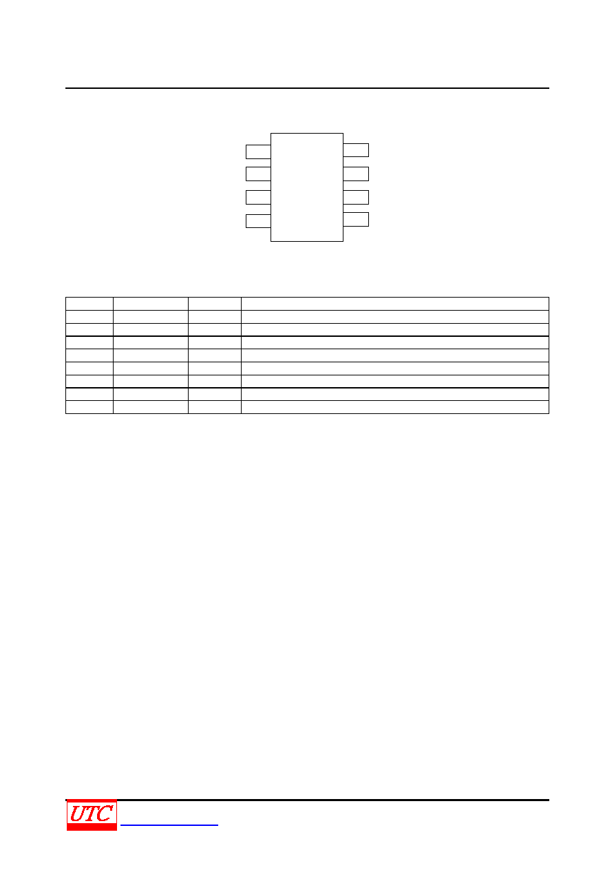
DIP - 8
SOP-8
*Pb - free plating product number: 3510L
ORDERING INFORMATION
Order Number
Normal
Lead Free Plating
Package Packing
3510-D08-T 3510L-D08-T
DIP-8 Tube
3510-S08-R 3510L-S08-R
SOP-8
Tape
Reel
3510-S08-T 3510L-S08-T
SOP-8
Tube
3510L- D08-T
(1)Packing Type
(2)Package Type
(3)Lead Plating
(1) R: Tape Reel, T: Tube
(2) D08: DIP-8, S08: SOP-8
(3) L: Lead Free Plating, Blank: Pb/Sn
3510
CMOS
IC
UNISONIC TECHNOLOGIES CO., LTD
2 of 9
www.unisonic.com.tw
QW-R502-048,B
PIN CONFIGURATION
PIN DESCRIPTION
PIN No.
PIN NAME
TYPE
DESCRIPTION
1
PGI
I
Power good input
2 GND
Ground
3
FPO
O
Fault protection output(invert), open drain output stage
4 PSON I
ON/OFF
control
5 V
S33
I
3.3V
over/under-voltage protection
6 V
S5
I
5V over/under-voltage protection
7 V
DD
I
Supply voltage/12V over-voltage protection input pin
8
PGO
O
Power good output, open drain output stage
PGO
V
DD
V
S5
V
S33
PSON
FPO
GND
PGI
4
3
2
1
8
7
6
5
3510
CMOS
IC
UNISONIC TECHNOLOGIES CO., LTD
3 of 9
www.unisonic.com.tw
QW-R502-048,B
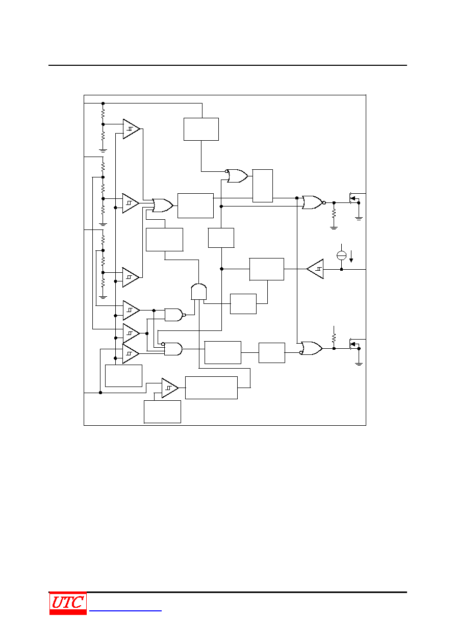
BLOCK DIAGRAM
POR
+
-
+
-
+
-
+
-
+
-
+
-
+
-
V
DD
V
S5
V
S33
PGI
Band - Gap
Reference
0.95 V
Band - Gap
Reference
1.2 V
150
s Debounce
and
4.8ms Delay
150
s
Debounce
PGI 2
PGI 1
300ms
Delay
PGO
V
DD
75ms
Delay
38ms
Debounce
PSON
FPO
V
DD
R
S
Q
73
s
Debounce
2.3ms
Delay
73
s
Debounce
5 V OV
12 V OV
3.3 V OV
3. 3 V UV
5 V UV
3510
CMOS
IC
UNISONIC TECHNOLOGIES CO., LTD
4 of 9
www.unisonic.com.tw
QW-R502-048,B
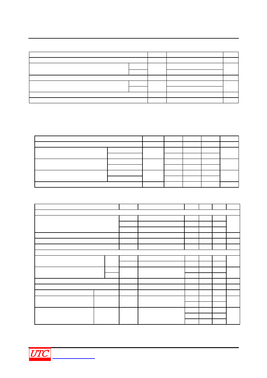
ABSOLUTE MAXIMUM RATINGS
PARAMETER SYMBOL
RATINGS
UNIT
Supply Voltage
V
DD
16 V
FPO
16
Output Voltage
PGO
V
OUT
8
V
All Other Pins
-0.3 ~ 16
V
DIP-8 1092
Power Dissipation (T
a
25∞C)
SOP-8
P
D
730
mWV
Operating Temperature
T
OPR
-20 ~ +85
Storage Temperature
T
STG
-40 ~ +150
Note: 1. Absolute maximum ratings are stress ratings only and functional device operation is not implied. The device
could be damaged beyond Absolute maximum ratings.
2. The device is guaranteed to meet performance specifications within 0 ~
+70 operating
temperature range
and assured by design from -20 ~
+85 .
RECOMMENDED OPERATING CONDITIONS
PARAMETER SYMBOL
MIN
TYP
MAX
UNIT
Supply Voltage
V
DD
4 15 V
PSON, VS5, VS33
7
Input Voltage
PGI
V
IN
V
DD
+0.3V 7
V
FPO
15
Output Voltage
PGO
V
OUT
7
V
FPO
20
Output Sink Current
PGO
I
O(SINK)
10
mA
Supply Voltage Rising Time (See Note)
1
ms
Note: V
DD
rising and falling slew rate must be less than 14V/ms.
ELECTRICAL CHARACTERISTICS
(T
a
=
25∞C ,unless otherwise specified.)
PARAMETER SYMBOL
TEST
CONDITIONS
MIN
TYP
MAX
UNIT
OVER-VOLTAGE PROTECTION
V
S33
3.7
3.9
4.1
V
S5
5.7
6.1
6.5
Over Voltage Threshold
V
DD
13.2
13.8
14.4
V
Low-level Output Voltage (FPO)
V
OL
V
DD
=5V, I
O(SINK)
=20mA
0.7
V
Leakage Current (FPO)
I
LEAK
V
(FPO)
=5V
5
µA
Noise Deglitch Time OVP
V
DD
=5V
35
73
110
µS
PGI AND PGO
V
PGI
1.1
1.15
1.2
Input threshold Voltage
PGI
V
PG2
0.9
0.95
1
V
V
S33
2 2.2 2.4
Under Voltage Threshold
V
S5
V
IT
3.3 3.5 3.7
V
Low-level Output Voltage (PGO)
V
OL
V
DD
=4V, I
O(SINK)
=10 mA
0.4
V
Leakage Current (PGO)
I
LEAK
PGO = 5 V
5
µA
Short-Circuit Protection Delay
3.3V, 5V
49
75
114
ms
200 300 450
Transient Delay time
PGI to PGO
PGI to FPO
t
DLY1
V
DD
= 5 V
3.2 4.8 7.2
ms
88 150 225
180 296 445
Noise Deglitch Time
PGI to PGO
PGI to FPO
UVP to FPO
V
DD
= 5 V
82 146 220
µs
3510
CMOS
IC
UNISONIC TECHNOLOGIES CO., LTD
5 of 9
www.unisonic.com.tw
QW-R502-048,B
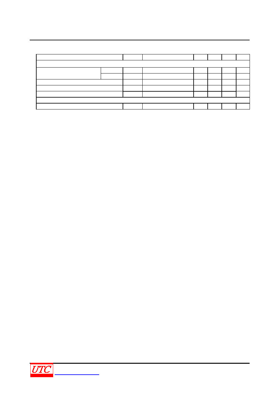
ELECTRICAL CHARACTERISTICS(Cont.)
PARAMETER SYMBOL
TEST
CONDITIONS
MIN
TYP
MAX UNIT
PSON CONTROL
High-level
V
IH
2.4
V
Input Voltage
Low-level
V
IL
1.2
V
Input Pullup Current
I
IN
PSON = 0 V
120
µA
Debounce Time (PSON)
t
B
V
DD
= 5 V
24
38
57
ms
Transient Delay Time (PSON to FPO)
t
DLY2
V
DD
= 5 V
t
B
+1.1 t
B
+2.3 t
B
+4
ms
TOTAL DEVICE
Supply Current
I
DD
PSON
=5V
1 mA