UTC 3511 CMOS IC
UTC
UNISONIC TECHNOLOGIES CO., LTD.
1
QW-R502-015,B
PC POWER SUPPLY
SUPERVISORS
DESCRIPTION
The UTC 3511 provides protection circuits, power
good output (PGO), fault protection latch (FPL_N),
and protection detector function (PDON_N) control.
It can minimize external components of switching
power supply systems in personal computer.
The Over Voltage Detector (OVD) monitors 3.3V,
5V, 12V input voltage level. The Under Voltage
Detector (UVD) monitors 3.3V, 5V input voltage level.
When OVD or UVD detect the fault voltage level, the
FPL_N is latched HIGH and PGO goes LOW. The
latch can be reset by PDON_N going HIGH. There is
2.4ms delay time for PDON_N turning off FPL_N.
When OVD and UVD detect the right voltage level,
the power good output (PGO) will be issue.
FEATURES
* The Over Voltage Detector (OVD) monitors
3.3V, 5V, 12V input voltage level.
* The Under Voltage Detector (UVD) monitors 3.3V,
5V input voltage level.
* Both of the power good output (PGO) and the fault
protection latch (FPL_N) are Open Drain Output.
* 75 ms time delay for UVD.
* 300 ms time delay for PGO.
* 38 ms for PDON_N input signal De-bounce.
* 73 us for internal signal De-glitches.
* 2.4 ms time delay for PDON_N turn-off FPL_N.
DIP-8
SOP-8
PIN CONFIGURATION
PGI
GND
FPL_N
PDON_N
V33
V5
VDD
PGO
1
2
3
4
8
7
6
5

UTC 3511 CMOS IC
UTC
UNISONIC TECHNOLOGIES CO., LTD.
2
QW-R502-015,B
PIN DESCRIPTION
PIN No.
PIN NAME
TYPE
DESCRIPTION
1 PGI
I
Power good input pin
2 GND
P Ground
3
FPL-N
O
Fault protection latch output pin (open drain output)
4
PDON-N
I
Protection detector function ON/OFF control input pin
5
V33
I
3.3V input pin
6
V5
I
5V input pin
7
VDD
I
Supply voltage/12V input pin
8
PGO
O
Power good output pin(open drain output)
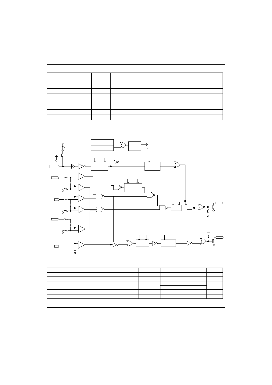
BLOCK DIAGRAM
PDON_N
V
DD
150uA
3.6V
Power On Reset
Vcc Low Voltage
POR
LVRST
Clock
Generator
CLK
PWR
V33
V5
V
DD
PGI
1.2V
UN
-
+
-
+
-
+
-
+
-
+
-
+
CLK RST
73us
debounce
CLK
CLR 300ms
delay
V
DD
PGO
FPL_N
R
S Q
CLK
RST
73us
debounce
CLR 75ms
delay
CLK
RWR
CLK
PWR
38ms
debounce
RST
CLK
PWR
2.4ms
delay
CLR
OV
OV
UN
OV
UN
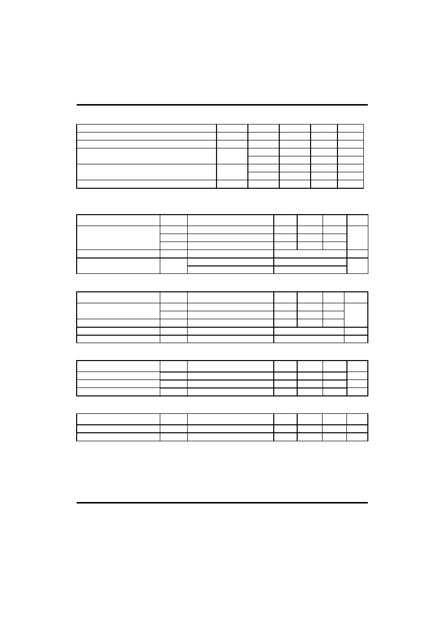
ABSOLUTE MAXIMUM RATINGS
PARAMETER
SYMBOL
RATINGS
UNIT
Supply voltage
V
DD
-0.3 ~ 16
V
Input Voltage PDON_N,V5,V33,PGI
Vin
-0.3 ~ 7
V
-0.3 ~ 16
Output Voltage
FPL_N
PGO
V
OUT
-0.3 ~ 7
V
Operating temperature
Topr
-40 ~ 125
�
C
Storage temperature
Tstg
-55 ~ 150
�
C
Note:Stresses above those listed may cause permanent damage to the devices

UTC 3511 CMOS IC
UTC
UNISONIC TECHNOLOGIES CO., LTD.
3
QW-R502-015,B
RECOMMENDED OPERATING CONDITIONS
PARAMETER
SYMBOL
MIN
TYP
MAX
UNIT
Supply Voltage
V
DD
3.8 12 15 V
Input Voltage PDON_N,V5,V33,PGI
Vin
7
V
15
V
Output Voltage
FPL_N
PGO
V
OUT
7
V
30
mA
Output Sink Current FPL_N
PGO
Iosink
10
mA
Supply Voltage Rising Time
Trs
1
ms
ELECTRICAL CHARACTERISTICS
(Ta=25
, V
DD
=5V)
Over Voltage Detection
PARAMETER SYMBOL
TEST
CONDITIONS MIN
TYP.
MAX
UNIT
V33
3.7 3.9 4.1
V5
5.7 6.1 6.5
Over voltage threshold
V
DD
/ V12
12.8
13.4 13.9
V
Leakage current (FPL_N)
I
LEAKAGE
FPL_N=5V
5 uA
I
sink
=10mA 0.3
Low level output voltage
(FPL_N)
V
OL
I
sink
=30mA 0.7
V
PGI and PGO
PARAMETER SYMBOL
TEST
CONDITIONS MIN
TYP.
MAX
UNIT
V33
2.55
2.69 2.83
Under voltage threshold
V5
4.1 4.3 4.47
Input threshold voltage (PGI)
V
PGI
1.16
1.20 1.24
V
Leakage current (PGO)
I
LEAKAGE
PGO=5V
5 uA
Low level output voltage (PGO)
V
OL
I
sink
=10mA 0.4
V
PDON_N
PARAMETER SYMBOL
TEST
CONDITIONS MIN
TYP.
MAX
UNIT
Input pull-up current
I
l
PDON_N=0V
150
uA
High-level input voltage
V
IH
2.4 V
Low-level input voltage
V
IL
1.2
V
TOTAL DEVICE
PARAMETER SYMBOL
TEST
CONDITIONS MIN
TYP.
MAX
UNIT
Supply current
Icc
PDON_N=5V
1
mA
low voltage
V
DD
3 V

UTC 3511 CMOS IC
UTC
UNISONIC TECHNOLOGIES CO., LTD.
4
QW-R502-015,B
SWITCHING CHARACTERISTICS, V
DD
=5V
PARAMETER SYMBOL
TEST
CONDITIONS MIN
TYP.
MAX
UNIT
De-bounce time (PDON_N)
t
db1
32 38 61 ms
Delay time (PGI to PGO)
t
delay
Ta=-40
�
C ~ 125
�
C
200 300 490 ms
De-bounce time (PDON_N)
t
db2
32 38 61 ms
De-glitch time
t
g
63 73 120 us
PDON_N to FPL_N delay time
t
delay2
T
db2
+2.0 T
db2
+2.4 T
db2
+3.8 ms
Internal UVD delay time
t
delay3
FPL_N go low & every
Time PGI>1.2V
65 75 122
ms
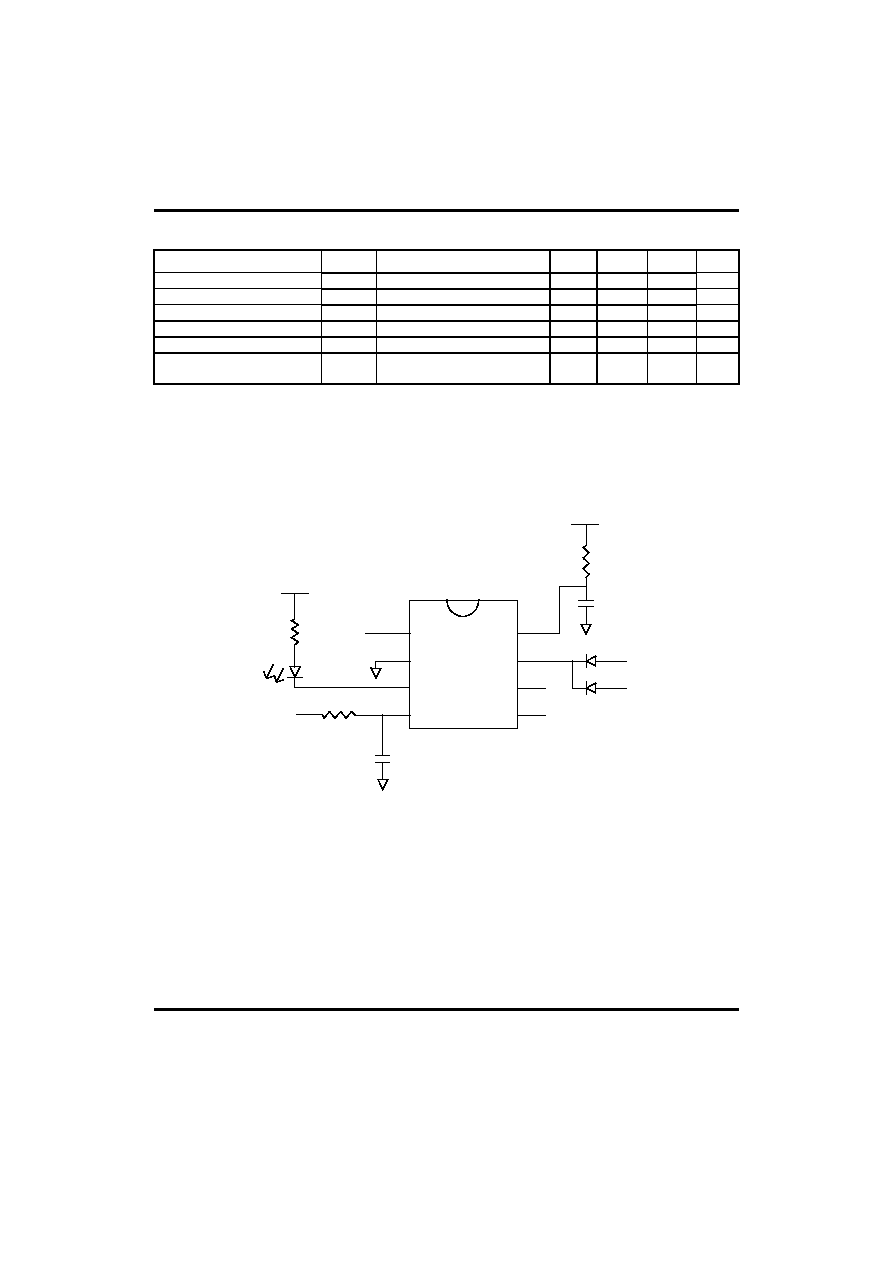
APPLICATION CIRCUIT
5V
PGI
470
PDON_N
0.01uF
1
2
3
4
8
7
6
5
0.01uF
5V
12V
VSB
PGI
GND
FPL_N
PDON_N
PGO
VDD
V5
V33
3511
3.3V
5V

UTC 3511 CMOS IC
UTC
UNISONIC TECHNOLOGIES CO., LTD.
5
QW-R502-015,B
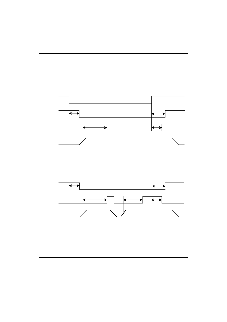
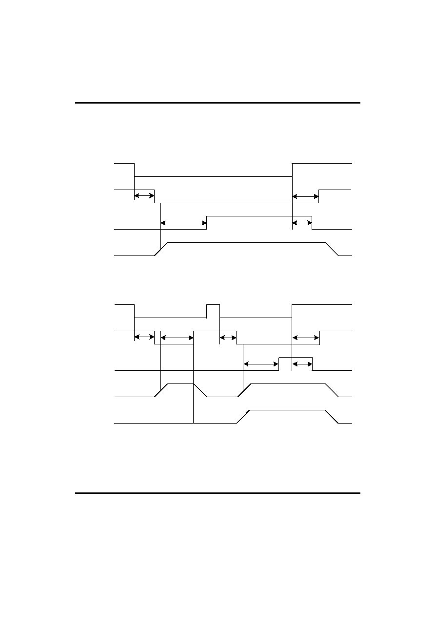
APPLICATION TIMMING
1. PGI
(UNDER_VOLTAGE):
PDON_N
FPL_N
PGO
PGI
t
db1
t
delay1+
t
g
t
delay2
t
db2
t
delay1+
t
g
PDON_N
FPL_N
PGO
PGI
t
db1
t
delay1+
t
g
t
delay2
t
db2

UTC 3511 CMOS IC
UTC
UNISONIC TECHNOLOGIES CO., LTD.
6
QW-R502-015,B
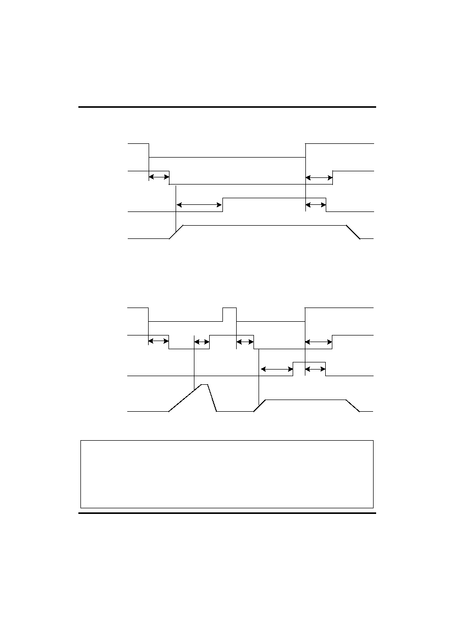
2. V33,V5
(UNDER_VOLTAGE):
PDON_N
FPL_N
PGO
PGI
t
db1
t
delay3+
t
g
t
delay2
t
db2
t
delay1+
t
g
V33 / V5
t
db1
t
delay3
=75mS
PDON_N
FPL_N
PGO
V33 / V5
t
db1
t
delay1+
t
g
t
delay2
t
db2

UTC 3511 CMOS IC
UTC
UNISONIC TECHNOLOGIES CO., LTD.
7
QW-R502-015,B
3. V33,V5,V12
(OVER_VOLTAGE):
PDON_N
FPL_N
PGO
t
db1
t
delay2
t
db2
t
delay1+
t
g
V33 / V5 / V12
t
g
t
db1
PDON_N
FPL_N
PGO
t
db1
t
delay1+
t
g
t
delay2
t
db2
V33 / V5 / V12
UTC assumes no responsibility for equipment failures that result from using products at values that
exceed, even momentarily, rated values (such as maximum ratings, operating condition ranges, or
other parameters) listed in products specifications of any and all UTC products described or contained
herein. UTC products are not designed for use in life support appliances, devices or systems where
malfunction of these products can be reasonably expected to result in personal injury. Reproduction in
whole or in part is prohibited without the prior written consent of the copyright owner. The information
presented in this document does not form part of any quotation or contract, is believed to be accurate
and reliable and may be changed without notice.

