 | –≠–ª–µ–∫—Ç—Ä–æ–Ω–Ω—ã–π –∫–æ–º–ø–æ–Ω–µ–Ω—Ç: 3563 | –°–∫–∞—á–∞—Ç—å:  PDF PDF  ZIP ZIP |

UTC 3563
LINEAR INTEGRATED CIRCUIT
UTC
UNISONIC TECHNOLOGIES CO., LTD.
1
QW-R103-013,B
HIGH-EFFICIENCY DC/DC
CONVERTER
DESCRIPTION
The UTC 3563 is a monolithic control circuit
containing the primary functions required for DC to DC
converters and highside-sensed constant current
source. The device consists of an internal temperature
compensated reference, comparator, controlled duty
cycle oscillator with an active current sense circuit,
bootstrapped driver, and high current output switch.
This device is specifically designed to construct a
constant current source for battery chargers with a
minimum number of external components.
Bootstrapped driver can drive the NPN output switch
to saturation for higher efficiency and less heat
dissipation. The UTC 3563 can deliver 1.5A
continuous current without requiring a heat sink.
FEATURES
*3V to 30V input voltage operation.
*Internal 2A peak current switch.
*1.5A continuous output current.
*Bootstrapped driver.
*High side current sense capability.
*High efficiency (up to 90%)
*Internal
±2% reference.
*Low quiescent current at 1.6mA.
*Frequency operation from 100Hz to 100KHz.
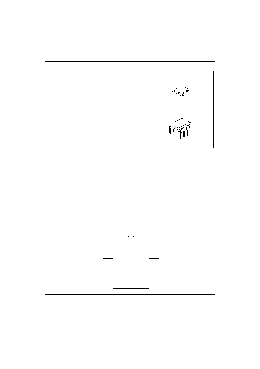
DIP-8
SOP-8
APPLICATIONS
*Constant current source for battery chargers.
*Saver for cellular phones.
*Step-Down DC-DC converter module.
PIN CONFIGURATION
DC
DE
CF
GND
BOOST
IS
VCC
FB
1
2
3
4
8
7
5
6

UTC 3563
LINEAR INTEGRATED CIRCUIT
UTC
UNISONIC TECHNOLOGIES CO., LTD.
2
QW-R103-013,B
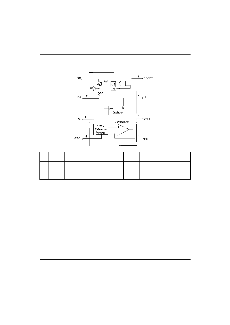
BLOCK DIAGRAM
PIN SYMBOL
DESCRIPTION
PIN SYMBOL
DESCRIPTION
1
DC
2A switch collector
5
FB
Feedback comparator inverting input
2
DE
Darlington switch emitter
6
VCC
Power supply input
3
CF
Oscillator timing capacitor
7
IS
Highside current sense input
(V
CC
-V
IS
=300mV)
4
GND
Power ground
8
BOOST Bootstrapped driver collector

UTC 3563
LINEAR INTEGRATED CIRCUIT
UTC
UNISONIC TECHNOLOGIES CO., LTD.
3
QW-R103-013,B
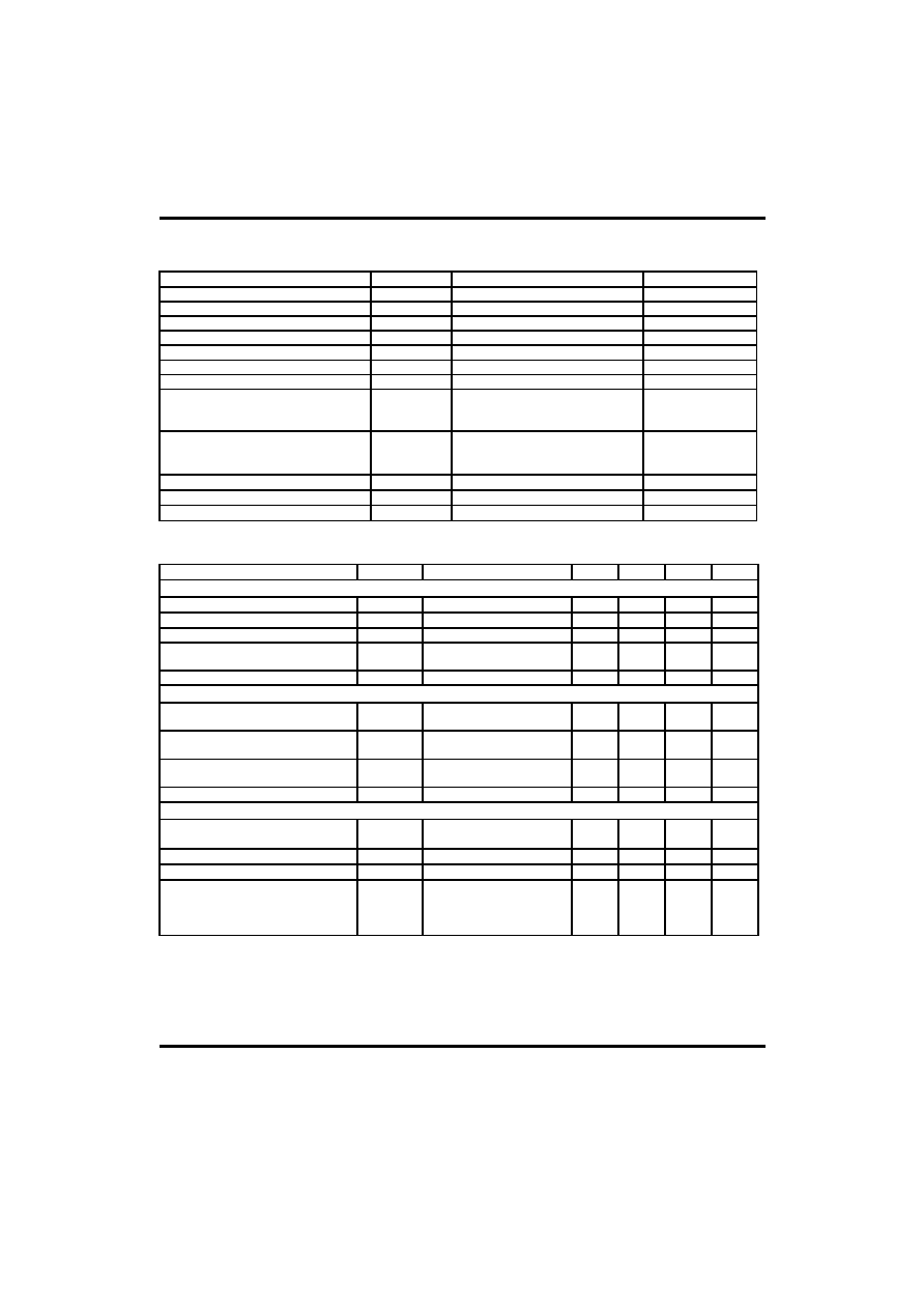
ABSOLUTE MAXIMUM RATINGS
(Ta=25
∞C)
PARAMETER
SYMBOL VALUE
UNIT
Supply Voltage
VCC
30
V
Comparator input voltage range
Vi
-0.3~+30
V
Switch collector voltage
V
C
(switch) 30
V
Switch emitter Voltage
V
E
(switch) 30
V
Switch collector to emitter voltage
V
CE
(switch) 30
V
Driver collector Voltage
V
C
(driver) 30
V
Switch current
I
SW
2
A
Power dissipation (Ta=25
∞C)
DIP-8
SOP-8
1000
625
mW
mW
Thermal Resistance
DIP-8
SOP-8
100
160
∞C/W
∞C/W
Operating junction temperature
Tj
125
∞C
Operating ambient temperature range
Ta
0~+70
∞C
Storage temperature range
Tstg
-65~+150
∞C
ELECTRICAL CHARACTERISTICS
(VCC=5.0V, Ta=25
∞C, unless otherwise specified)
PARAMETER SYMBOL
TEST
CONDITIONS
MIN
TYP.
MAX
UNIT
Oscillator
Charging Current
I
CHG
5V
VCC30V
10 25 40
µA
Discharging Current
I
DISCHG
5V
VCC30V
100 150 200
µA
Voltage Swing
Vosc
PIN 3
0.6
V
Discharge to Charge Current Ratio I
DISCHG
/
I
CHG
V
IS
=VCC
6.0
Current limit Sense Voltage
VCC -V
IS
I
CHG
=I
DISCHG
250 300 350 mV
Output Switch
Saturation Voltage,
Emitter Follower Connection
V
CE(SAT)
I
DE
=1.0A,
V
BOOST
=V
DC
=VCC
1.5
1.8 V
Saturation Voltage
V
CE(SAT)
I
DC
=1.0A, I
BOOST
=50mA,
(Forced
20)
0.4
0.7 V
DC Current Gain
h
FE
I
SC
=1.0A
V
CE
=5.0V
35 120
Collector Off State Current
I
C(OFF)
V
CE
=30V
10 nA
Comparator
Threshold Voltage
V
FB
Ta=25
∞C
0
∞CTa70∞C
1.225
1.210
1.250 1.275
1.290
V
V
Threshold voltage Line Regulation REG
LINE
3V
VCC30V
0.1
0.3
mV/V
Input Bias Current
I
IB
V
IN
=0V
0.4
1.0
µA
Supply Current
ICC
V
IS
=VCC, PIN 5>V
FB
,
5.0V
VCC30V, C
T
=1nF,
PIN 2=GND, Remaining
pins open
1.6
3.0
mA

UTC 3563
LINEAR INTEGRATED CIRCUIT
UTC
UNISONIC TECHNOLOGIES CO., LTD.
4
QW-R103-013,B
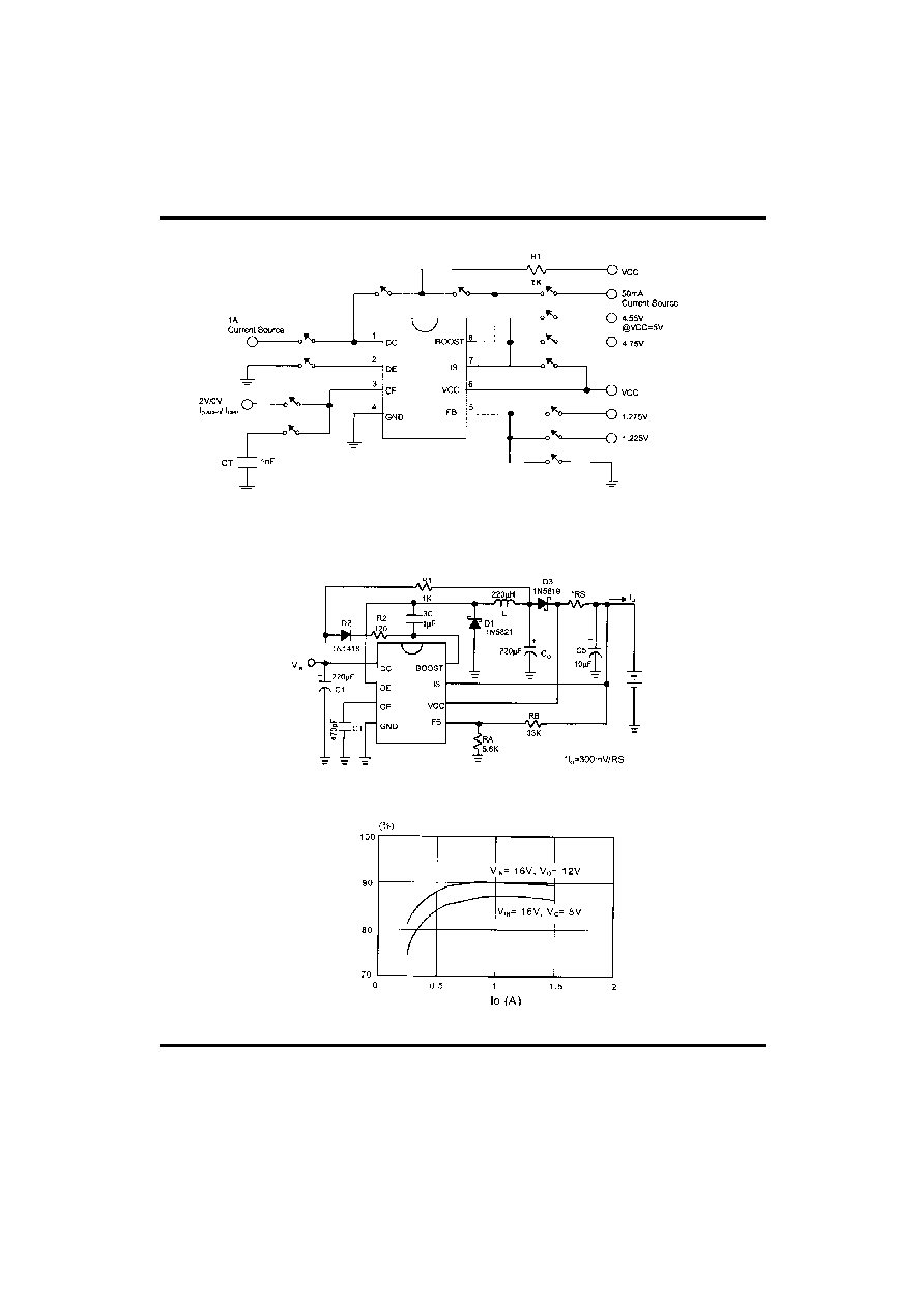
TEST CIRCUIT
TYPICAL APPLICATION CIRCUIT
EFFICIENCY vs OUTPUT CURRENT

UTC 3563
LINEAR INTEGRATED CIRCUIT
UTC
UNISONIC TECHNOLOGIES CO., LTD.
5
QW-R103-013,B
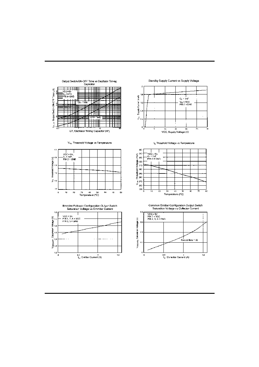
TYPICAL PERFORMANCE CHARACTERISTICS

UTC 3563
LINEAR INTEGRATED CIRCUIT
UTC
UNISONIC TECHNOLOGIES CO., LTD.
6
QW-R103-013,B
APPLICATION INFORMATION
DESIGN FORMULA TABLE
CALCULATION STEP-DOWN
STEP-UP
t
ON
/t
OFF
V
OUT
+V
F
V
IN(MIN)
-V
SAT
-V
OUT
V
OUT
+V
F
-V
IN(MIN)
V
IN(MIN)
-V
SAT
(t
ON
+t
OFF
)
MAX
1/F
MIN
1/F
MIN
C
T
4x10
-5
t
ON
4x10
-5
t
ON
I
C(SWITCH)
2I
OUT(MAX)
t
ON
+ t
OFF
2I
OUT(MAX)
( )
t
OFF
RS 0.3/I
C(SWITCH)
0.3/I
C(SWITCH)
L(MIN)
V
IN(MIN)
-V
SAT
-V
OUT
( ) t
ON(MAX)
I
C(SWITCH)
V
IN(MIN)
- V
SAT
( ) t
ON(MAX)
I
C(SWITCH)
Co
I
C(SWITCH)
(t
ON
+t
OFF
)
8V
RIPPLE(P-P)
I
OUT
t
ON
V
RIPPLE(P-P)
V
SAT
: Saturation voltage of the output switch
V
F
: Forward voltage of the ringback rectifier
The following power supply characteristics must be chosen:
V
IN
: Norminal input voltage
V
OUT
: Desired output voltage, V
OUT
=1.25(1+RB/RA)
I
OUT
: Desired output current
F
MIN
: Minimum desired switching frequency at selected values for V
IN
AND I
OUT
V
RIPPLE(P-P)
: Desired peak-to-peak output ripple voltage. In practice, the calculated value will need to be increased
due to the capacitor equivalent series resistance and board layout. The ripple voltage should be kept to
a low value since it will directly affect the line and load regulation.
APPLICATION EXAMPLES
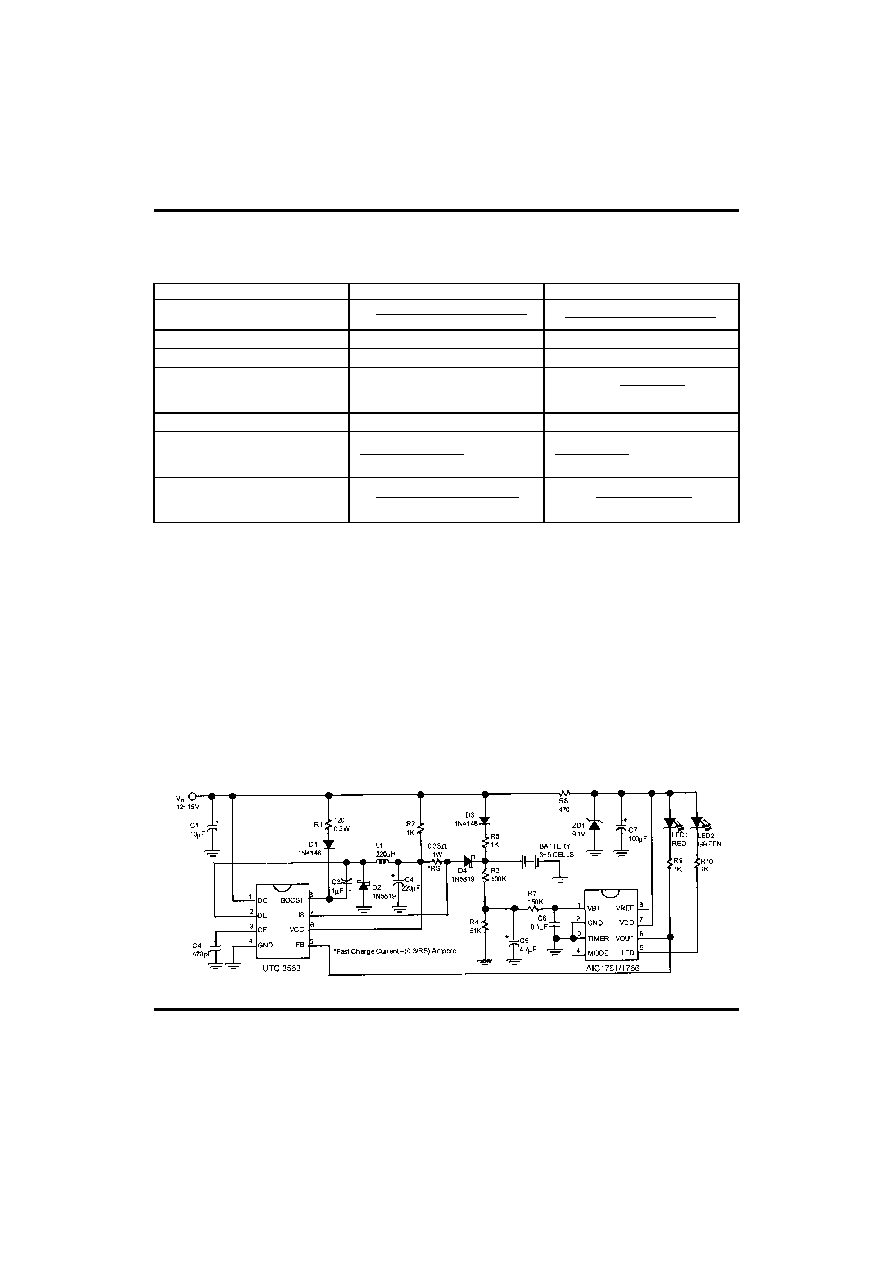
Fig. 1 Simplified Battery Charge Circuit for Ni-Cd/Ni-MH Battery

UTC 3563
LINEAR INTEGRATED CIRCUIT
UTC
UNISONIC TECHNOLOGIES CO., LTD.
7
QW-R103-013,B
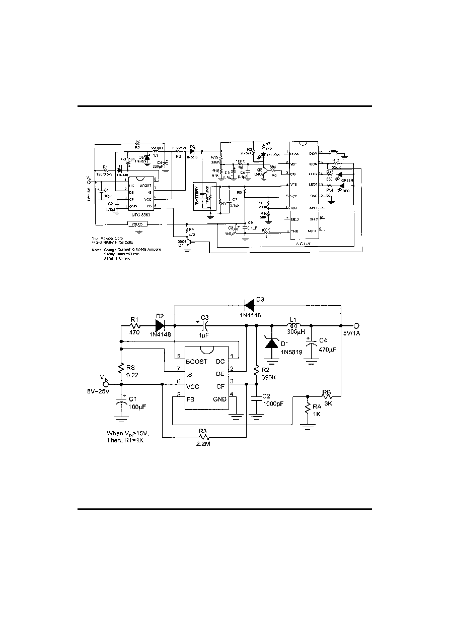
Fig.2 Battery Charge Circuit for Fluctuating Charging Current Applications
Fig. 3 Step-Down Converter
Line regulation: 40mV (V
IN
=10V~20V, @I
O
=1A)
Load regulation: 20mV (V
IN
=15V, @I
O
=100mA~1A)
Short circuit current: 1.3A (V
IN
=15V, @R
L
=0.1
)

UTC 3563
LINEAR INTEGRATED CIRCUIT
UTC
UNISONIC TECHNOLOGIES CO., LTD.
8
QW-R103-013,B
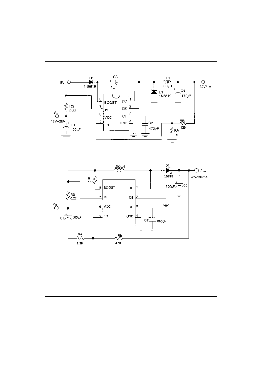
Fig. 4 Step-Down Converter with External 5V Bootstrap
Fig. 5 Step-Up Converter
Line regulation: 100mV (V
IN
=8V~16V, @Io=200mA)
Load regulation: 40mV (V
IN
=12V, @I
O
=80mA~200mA)

UTC 3563
LINEAR INTEGRATED CIRCUIT
UTC
UNISONIC TECHNOLOGIES CO., LTD.
9
QW-R103-013,B
Fig. 6 Step-Up Converter with External NPN Switch
Fig. 7 Inverting Converter
Line regulation: 20mV (V
IN
=4.5V~6V, @I
O
=100mA)
Load regulation: 100mV (V
IN
=5V, @I
O
=10mA~100mA)

UTC 3563
LINEAR INTEGRATED CIRCUIT
UTC
UNISONIC TECHNOLOGIES CO., LTD.
10
QW-R103-013,B
UTC assumes no responsibility for equipment failures that result from using products at values that
exceed, even momentarily, rated values (such as maximum ratings, operating condition ranges, or
other parameters) listed in products specifications of any and all UTC products described or contained
herein. UTC products are not designed for use in life support appliances, devices or systems where
malfunction of these products can be reasonably expected to result in personal injury. Reproduction in
whole or in part is prohibited without the prior written consent of the copyright owner. The information
presented in this document does not form part of any quotation or contract, is believed to be accurate
and reliable and may be changed without notice.
