 | –≠–ª–µ–∫—Ç—Ä–æ–Ω–Ω—ã–π –∫–æ–º–ø–æ–Ω–µ–Ω—Ç: 4052 | –°–∫–∞—á–∞—Ç—å:  PDF PDF  ZIP ZIP |
UTC 4052 CMOS
UTC
UNISONIC TECHNOLOGIES CO., LTD.
1
QW-R502-013,A
ANALOG MULTIPLEXERS
/DEMULTIPLEXERS
DESCRIPTION
The UTC 4052 analog multiplexers is digitally
≠controlled analog switch. The device feature low ON
impedance and very low OFF leakage current. Control
of analog signals up to the complete supply voltage
range can be achieved.
FEATURES
*Triple Diode Protection on Control Inputs
*Switch Function is Break Before Make
*Supply Voltage Range=3.0 Vdc to 18 Vdc
*Analog Voltage Range(VDD-VEE)=3.0 to 18V
*
Note:VEE must beVss
*Linearized Transfer Characterisstics
*Low-noise-12nV/Cycle ,f1.0kHz Typical
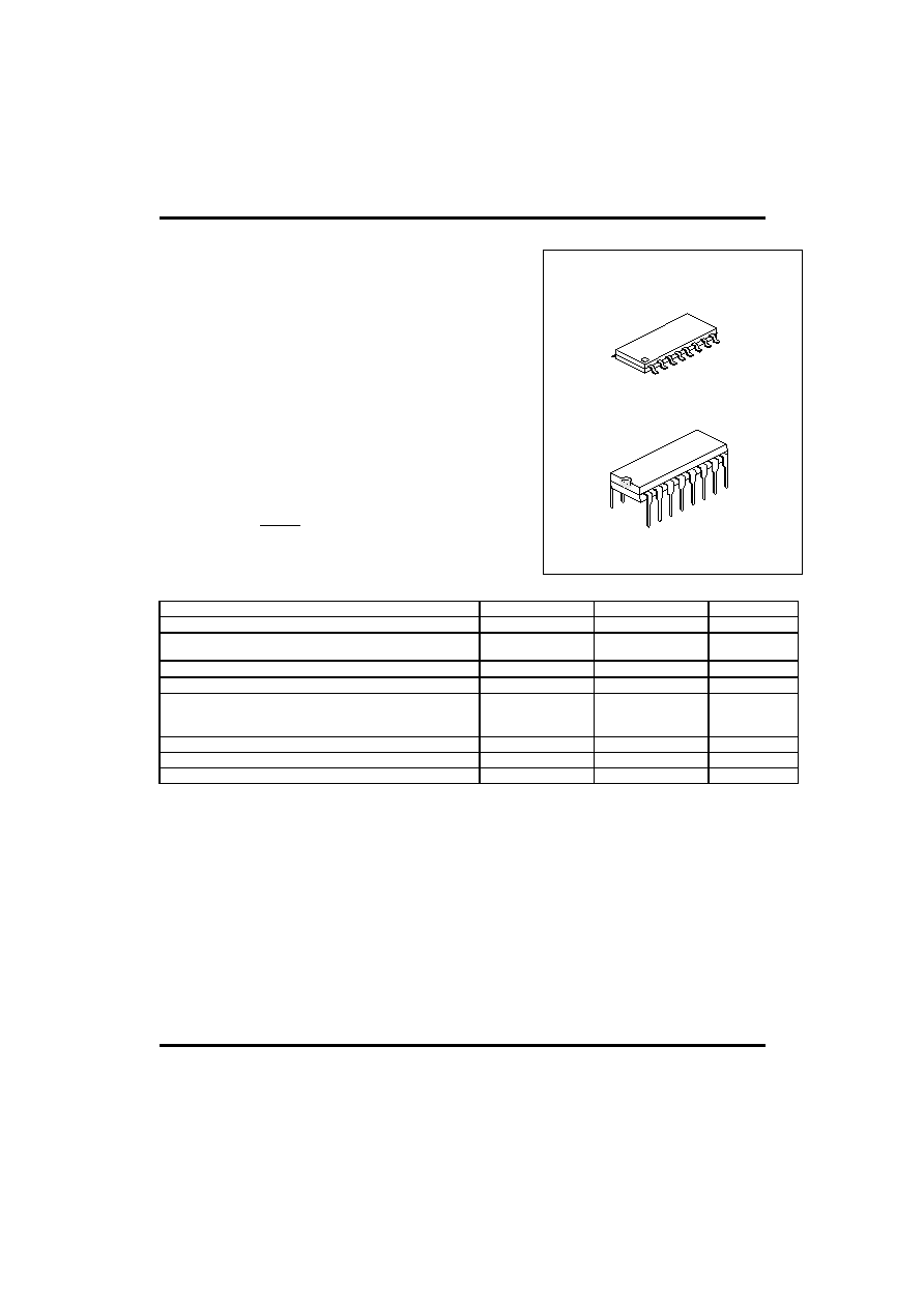
DIP-16
SOP-16
ABSOLUTE MAXIMUM RATINGS*
1
PARAMETER
SYMBOL
RATING
UNIT
DC Supply Voltage (Referenced to V
EE
,VssV
EE
)
V
DD
-0.5 ~ +18.0
V
Input or Output Voltage (DC or Transient) (Referenced to
Vss for Control Inputs and V
EE
for switch I/O)
Vin,Vout
-0.5 ~ V
DD
+0.5
V
Input Current (DC or Transient) per Control Pin
Iin
±
10
mA
Switch Through Current
I
SW
±
25
mA
Power Dissipation *
2
DIP-16
SOP-16
P
D
700
500
mW
Ambient Temperature Range
T
A
-55 ~ +125
∞C
Storage Temperature Range
Tstg
-65 ~ +150
∞C
Lead Temperature (8-Second Soldering)
T
LEAD
260
∞C
*1. Maximum Ratings are those values beyond which damage to the device may occur.
*2. Temperature Derating : 7.0 mW/ From 65 ~ 125
UTC 4052 CMOS
UTC
UNISONIC TECHNOLOGIES CO., LTD.
2
QW-R502-013,A
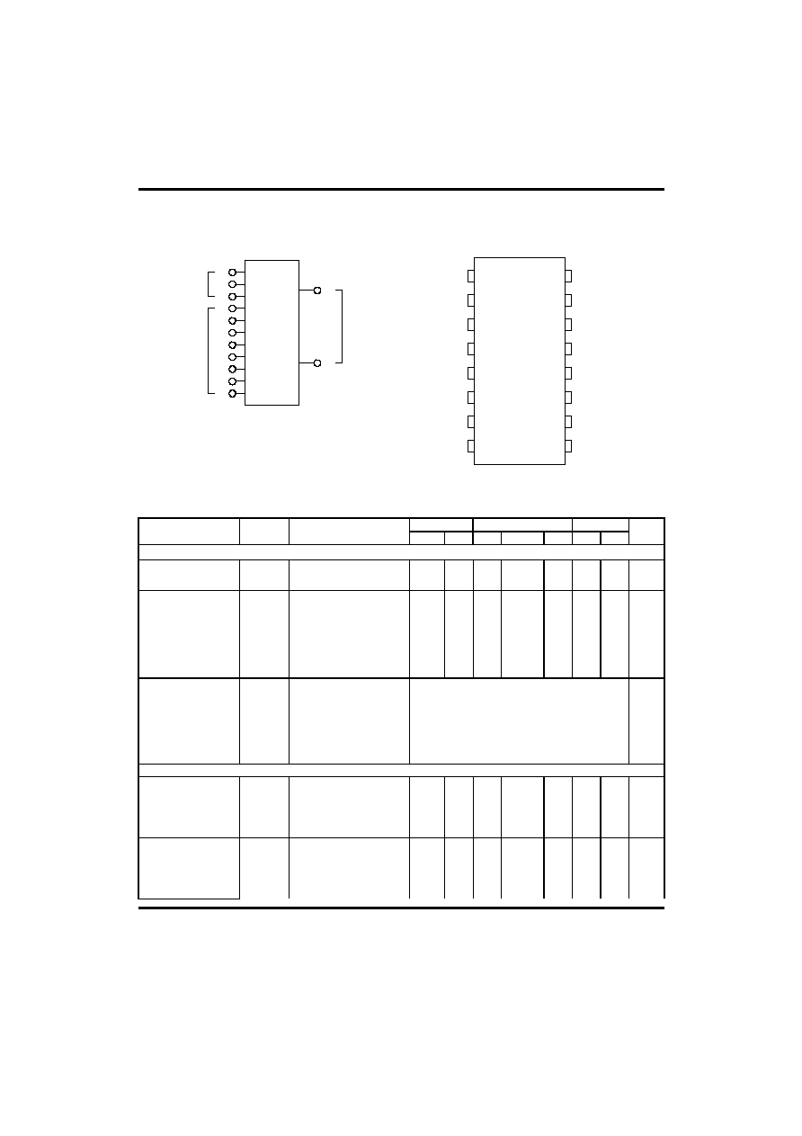
INHIBIT
A
B
X0
X1
X2
X3
Y0
Y1
Y2
Y3
6
10
9
12
14
15
11
1
5
2
4
X
Y
Dual 4-Channel Analog
Multiplexer/Demultiplexer
CONTROLS
SWITCHES
IN/OUT
COMMONS
OUT/IN
13
9
V
DD
=PIN16, V
SS
=PIN8, V
EE
=PIN7
1
2
3
4
5
6
7
8
Y0
Y2
Y
Y3
Y1
INH
V
EE
Vss
9
10
11
12
13
14
15
16
V
DD
X2
X1
X
X0
X3
A
B
PIN ASSIGMENT
Note: Control Inputs referenced to Vss.
Analog Inputs and Outputs reference to VEE.
VEE must be <Vss.
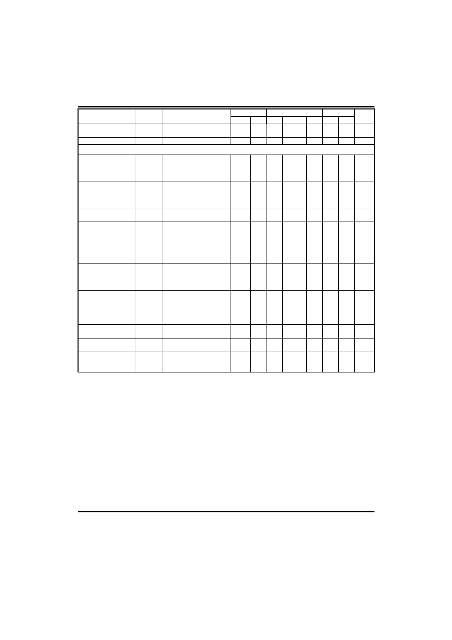
ELECTRICAL CHARACTERISTICS
-55∞C 25∞C 125∞C
PARAMETER SYMBOL TEST
CONDITIONS
MIN MAX MIN TYP
*3
MAX MIN MAX
UNIT
SUPPLY REQUIREMENTS (Voltages Referenced to VEE)
Power Current Per
Range
V
DD
V
DD
-3.0VssV
EE
3.0 18
3.0
18 3.0 18 V
Quiescent Current
Per Package
I
DD
Control
Inputs:
Vin=Vss or V
DD
,Switch
I/O : V
EE
V
I/O
V
DD,
andVswitch500mV
*4
V
DD
=5.0V
V
DD
=10V
V
DD
=15V
5.0
10
20
0.005
0.010
0.015
5.0
10
20
150
300
600
µA
Total Supply Current
(Dynamic Plus
Quiescent, Per
Package
I
D(AV)
TA=25only (The
channel component,
(Vin-Vout) /Ron, is not
included.)
V
DD
=5.0V
V
DD
=10V
V
DD
=15V
(0.07µA/kHz)f+I
DD
Typical (0.20µA/kHz)f+I
DD
(0.36µA/kHz)f+I
DD
µA
CONTROL INPUTS-INHIBIT, A, B, C (Voltages Referenced to Vss)
Low-Level Input
Voltage
V
IL
Ron=per
spec,
Ioff=per spec
V
DD
=5.0V
V
DD
=10V
V
DD
=15V
1.5
3.0
4.0
2.25
4.50
6.75
1.5
3.0
4.0
1.5
3.0
4.0
V
High-Level Input
Voltage
V
IH
Ron=per
spec,
Ioff=per spec
V
DD
=5.0V
V
DD
=10V
V
DD
=15V
3.5
7.0
11
3.5
7.0
11
2.75
5.50
8.25
3.5
7.0
11
-
-
-
V
UTC 4052 CMOS
UTC
UNISONIC TECHNOLOGIES CO., LTD.
3
QW-R502-013,A
-55∞C 25∞C 125∞C
PARAMETER SYMBOL TEST
CONDITIONS
MIN MAX MIN TYP
*3
MAX MIN MAX
UNIT
Input Leakage
Current
Iin
V
DD
=15V ,Vin=0 or
V
DD
±
0.1
±
10
-5
±
0.1
1.0 µA
Input
Capacitance Cin
5.0
7.5
pF
SWITCHES IN/OUT AND COMMONS OUT/IN ≠X,Y,Z(Voltages Referenced to V
EE
)
Recommended
Peak-to-Peak
Voltage Into or Out of
the Switch
V
I/O
Channel On or Off
0
V
DD
0
V
DD
0 V
DD
Vpp
Recommended Static
or Dynamic Voltage
Across the Switch *
4
(Figure 3)
V
switch
Channel On
0
600
0
600
0
300
mV
Output Offset
Voltage
Voo
Vin=0V,No
Load
10 µV
ON Resistance
Ron
V
switch
500mV *
4
Vin=V
IL
or V
IH
(Control),
and Vin=0 to V
DD
(Switch)
V
DD
=5.0V
V
DD
=10V
V
DD
=15V
800
400
220
250
120
80
1050
500
280
1200
520
300
ON Resistance
Between Any Two
Channels in the
Same Package
Ron V
DD
=5.0V
V
DD
=10V
V
DD
=15V
70
50
45
25
10
10
70
50
45
135
95
65
Off-Channel Leakage
Current(Figure 8)
Ioff
V
DD
=15V ,Vin=VIL or VIH
(Control) Channel to
Channel or Any One
Channel
±
100
±
0.05
±
100
±
1000
nA
Capacitance,
Switch I/O
C
I/O
Inhibit=V
DD
10 pF
Capacitance,
Common O/I
C
O/I
Inhibit=V
DD
32 pF
Capacitance,
Feedthrough
(Channel Off)
C
I/O
Pins Not Adjacent
Pins Adjacent
0.15
0.47
pF
*3. Data labeled "Typ" is not to be used for design purposes, but is intended as an indication of the IC's potential
*
performance.
*4. For voltage drops across the switch (Vswitch) > 600 mV ( > 300 mV at high temperature), excessive V
DD
*
current may be drawn, i.e. the current out of the switch may contain both V
DD
and switch input components. The
*
reliability of the device will be unaffected unless the Maximum Ratings are exceeded. (See first page of this data
*
sheet.)
UTC 4052 CMOS
UTC
UNISONIC TECHNOLOGIES CO., LTD.
4
QW-R502-013,A
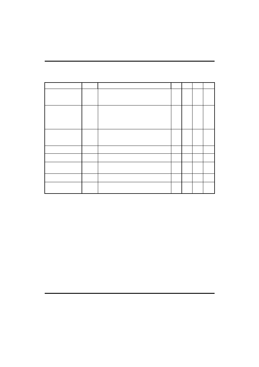
ELECTRICAL CHARACTERISTICS
*5
(C
L
= 50 pF, T
A
= 25) (V
EE
V
SS
unless otherwise indicated)
PARAMETER SYMBOL
TEST
CONDITIONS
MIN
TYP
*6
MAX UNIT
Propagation Delay
Times(Figure 4)
Switch Input to Switch
Output
t
PLH
,t
PHL
R
L
=10k
V
DD
-V
EE=
5.0, t
PLH
,t
PHL
=(0.17 ns/pF) C
L
+21.5 ns
V
DD
-V
EE=
10, t
PLH
,t
PHL
=(0.08 ns/pF) C
L
+8.0 ns
V
DD
-V
EE=
15, t
PLH
,t
PHL
=(0.06 ns/pF) C
L
+7.0 ns
30
12
10
75
30
25
ns
Propagation Delay
Times(Figure 4)
Inhibit to Output
t
PHZ
,t
PLZ
t
PZH
,t
PZL
RL=10k,VEE=Vss
Output"1" or "0" to High Impedance, or
High Impedance to"1" or "0" Level
V
DD
-V
EE=
5.0
V
DD
-V
EE=
10
V
DD
-V
EE=
15
300
155
125
600
310
250
ns
Propagation Delay
Times(Figure 4)
Control Input to Output
t
PLN
,t
PHL
RL=10k,V
EE
=Vss
V
DD
-V
EE=
5.0
V
DD
-V
EE=
10
V
DD
-V
EE=
15
325
130
90
650
260
180
ns
Second Harmonic
Distortion
R
L
=10k, f=1kHz, V
in
=5Vpp,
V
DD
-V
EE=
10
0.07 %
Bandwidth (Figure 5)
BW
R
L
=1k, V
in
=1/2(V
DD
-V
EE
)p-p, C
L
=50pF,
20 Log (V
out
/V
in
)=-3dB,
V
DD
-V
EE=
10
17
MHz
Off Channel
Feedthrough Attenuation
(Figure 5)
R
L
=1k, Vin=1/2(V
DD
-V
EE
)p-p, Fin=30MHz,
V
DD
-V
EE=
10
-50
dB
Channel Separation
(Figure 6)
RL=1k, Vin=1/2(V
DD
-V
EE
)p-p, fin=3.0MHz
,
V
DD
-V
EE=
10
-50
dB
Crosstalk ,Control Input
to Common O/I (Figure
7)
R1=1k, R
L
=10k,
Control t
TLH
=t
THL
=20ns ,Inhibit=Vss),
V
DD
-V
EE=
10
75
mV
*5. The formulas given are for the typical characteristics only at 25 .
*6. Data labelled "Typ" is not lo be used for design purposes but In intended as an indication of the IC's potential
*
performance.
UTC 4052 CMOS
UTC
UNISONIC TECHNOLOGIES CO., LTD.
5
QW-R502-013,A
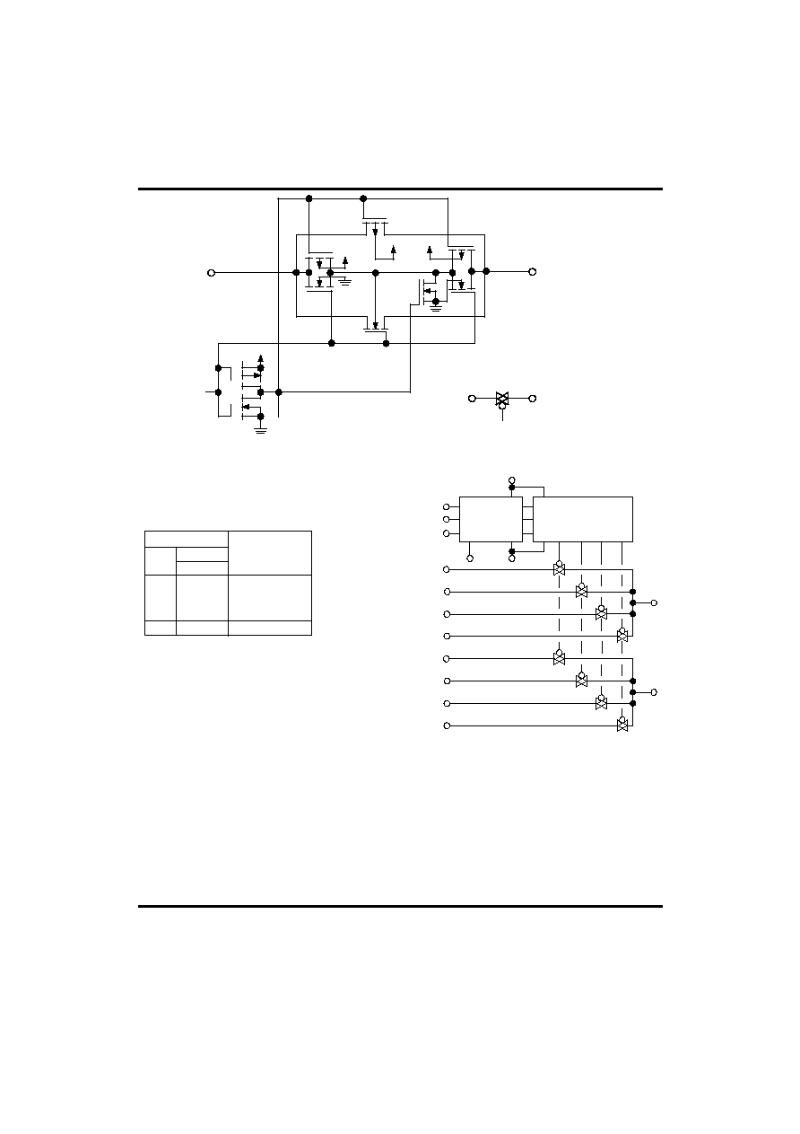
CONTROL
IN/OUT
OUT/IN
V
EE
LEVEL
CONVERTED
CONTROL
V
DD
IN/OUT
OUT/IN
V
DD
V
DD
V
DD
V
EE
Figure 1.Switch Circuit Schematic
TRUTH TABLE
Control Inputs
Inhibit
B A
Select
ON Switches
0
0
0
0
0
0
1
1
0
1
0
1
Y0
Y1
Y2
Y3
X0
X1
X2
X3
1
X
X
None
LEVEL
CONVERTER
BINARY TO 1-OF-4
DECODER WITH
INHIBIT
Figure 2. Functional Diagram
Y0
Y1
Y2
Y3
X0
X1
X2
X3
12
5
2
4
14
15
11
1
INH
A
B
6
10
9
8
Vss 7
V
EE
13
3
X
Y
16
V
DD
* X=Don't Care
TEST CIRCUITS