 | –≠–ª–µ–∫—Ç—Ä–æ–Ω–Ω—ã–π –∫–æ–º–ø–æ–Ω–µ–Ω—Ç: 4053 | –°–∫–∞—á–∞—Ç—å:  PDF PDF  ZIP ZIP |
UTC 4053 CMOS IC
UTC
UNISONIC TECHNOLOGIES CO., LTD.
1
www.unisonic.com.tw
QW-R502-036,A
ANALOG MULTIPLEXERS/ DEMULTIPLEXERS
DESCRIPTION
The UTC 4053 are Triple SPDT analog multiplexers for
application as digitally≠controlled analog switches.
FEATURES
* Analog Voltage Range (V
DD
≠ V
EE
) = 3.0 ~ 18 V
Note: V
EE
must beV
SS
* Linearized Transfer Characteristics
* Pin≠to≠Pin Replacement for CD4053
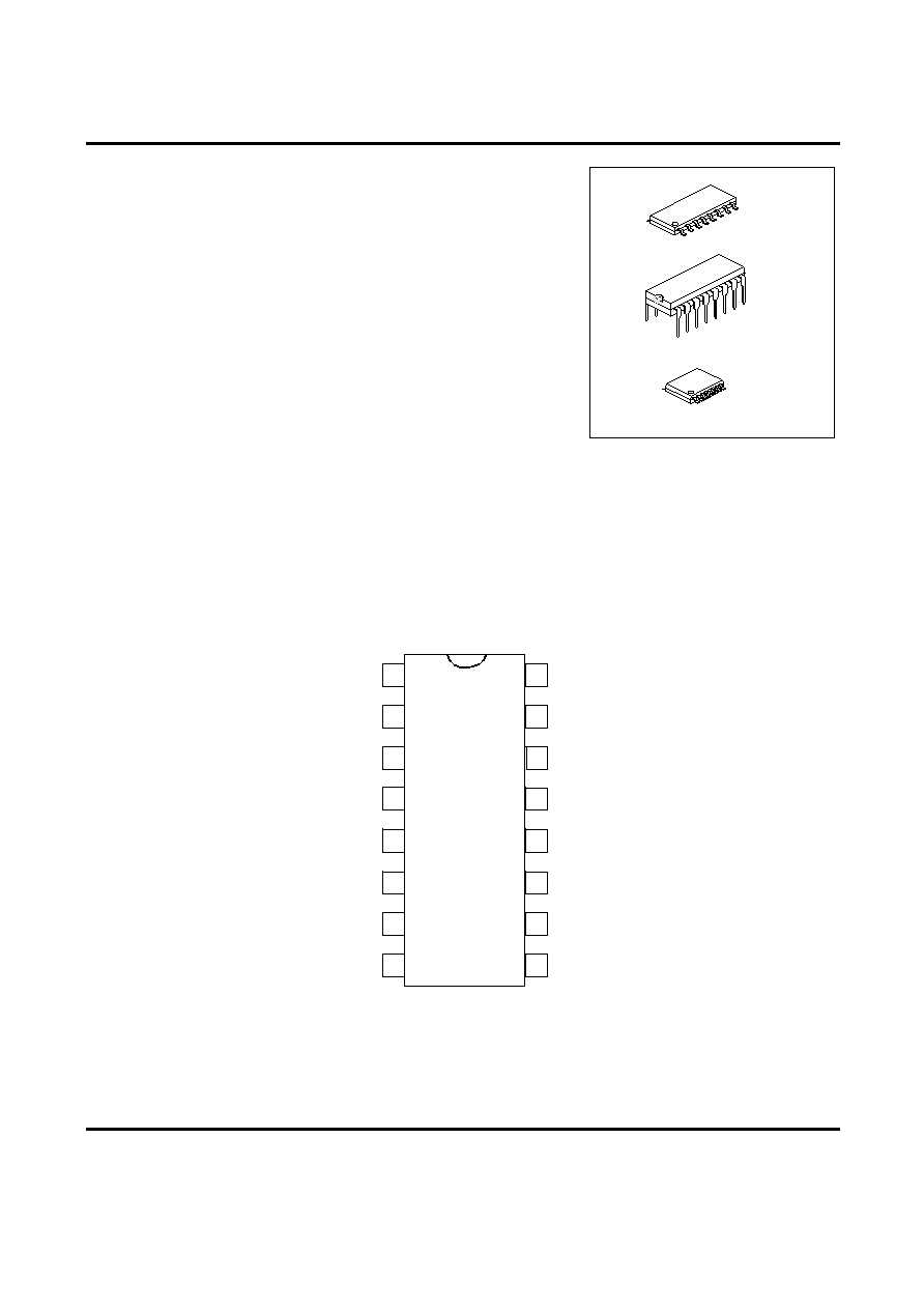
DIP-16
SOP-16
TSSOP-16
*Pb-free plating product number: 4053L
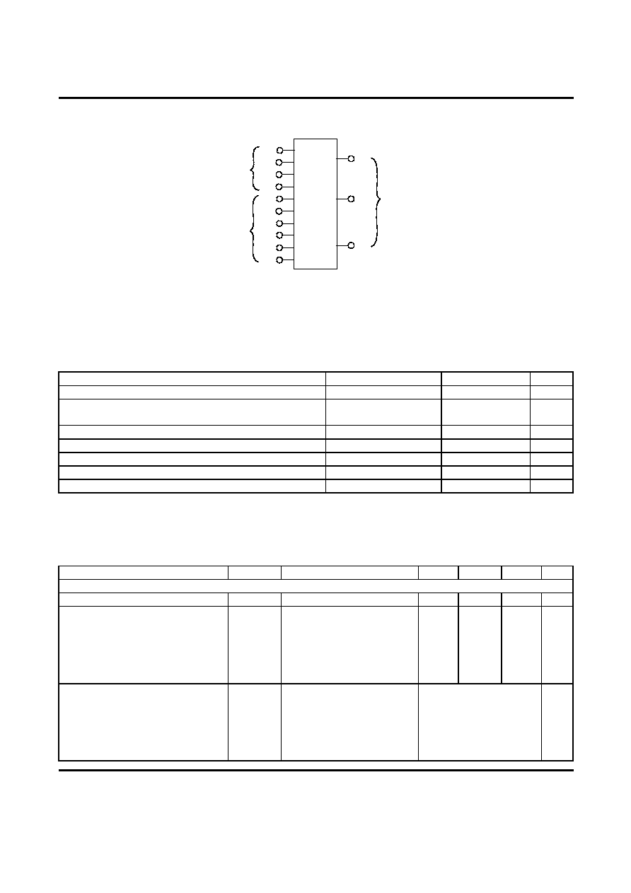
PIN CONFIGURATIONS
Z
1
Y
1
1
2
3
4
5
6
7
8
16
15
14
13
12
11
10
9
Y
0
Z
Z
0
INH
V
EE
V
SS
X
V
DD
Y
X
1
X
0
A
B
C
UTC 4053
UTC 4053 CMOS IC
UTC
UNISONIC TECHNOLOGIES CO., LTD.
2
www.unisonic.com.tw
QW-R502-036,A
UTC 4053 Triple 2≠Channel Analog Multiplexer/Demultiplexer
6
INHIBIT
C
X1
Y1
Z1
11
10
9
12
13
2
1
5
3
Z0
Y0
X0
B
A
14
15
4
Z
Y
X
COMMONS
OUT/IN
V
DD
= PIN 16
V
SS
= PIN 8
V
EE
= PIN 7
CONTROLS
SWITCHES
IN/OUT
Note: Control Inputs referenced to V
SS
, Analog Inputs and Outputs reference to V
EE
. V
EE
must beV
SS
.
ABSOLUTE MAXIMUM RATINGS*
PARAMETER SYMBOL
RATINGS
UNIT
DC Supply Voltage (Referenced to V
EE
, V
SS
V
EE
)
V
DD
-0.5 ~ +18.0
V
Input or Output Voltage (DC or Transient) (Referenced to V
SS
for Control Inputs and V
EE
for Switch I/O)
V
in
, V
out
-0.5 ~ V
DD
+0.5
V
Input Current (DC or Transient), per Control Pin
I
in
±10
mA
Switch Through Current
I
SW
±25
mA
Power Dissipation. Per Package**
P
D
500
mW
Storage Temperature
T
stg
-65 ~ +150
Lead Temperature (8 - Second Soldering)
T
Lead
260
* Maximum Ratings are those values beyond which damage to the device may occur.
** Temperature Derating: "DIP and SOP" Packages: ≠ 7.0 mW/ From 65 ~ 125
ELECTRICAL CHARACTERISTICS
(Ta=25, unless otherwise indicated.)
PARAMETER SYMBOL
TEST
CONDITIONS
MIN
TYP#
MAX
UNIT
SUPPLY REQUIREMENTS (Voltages Referenced to V
EE
)
Power Supply Voltage Range
V
DD
V
DD
≠ 3.0V
SS
V
EE
3.0 18
V
Quiescent Current per Package
I
DD
Control Inputs: Vin = V
SS
or V
DD
Switch I/O: V
EE
V
I/O
V
DD
,
and Vswitch500mV*
V
DD
=5.0V
V
DD
=10V
V
DD
=15V
0.005
0.010
0.015
5.0
10
20
µA
Total Supply Current (Dynamic Plus
Quiescent, Per Package)
I
D(AV)
T
a
=25 only (The channel
component, (Vin - Vout)/Ron, is
not included.)
V
DD
=5.0V
V
DD
=10V
V
DD
=15V
(0.07 µA/kHz) f + I
DD
Typical
(0.20 µA/kHz) f + I
DD
(0.36 µA/kHz) f + I
DD
µA
UTC 4053 CMOS IC
UTC
UNISONIC TECHNOLOGIES CO., LTD.
3
www.unisonic.com.tw
QW-R502-036,A
PARAMETER SYMBOL
TEST
CONDITIONS
MIN
TYP#
MAX
UNIT
CONTROL INPUTS ≠ INHIBIT A, B, C (Voltages Referenced to V
SS
)
Low ≠ Level Input Voltage
V
IL
Ron= per spec, Ioff = per spec
V
DD
=5.0V
V
DD
=10V
V
DD
=15V
2.25
4.50
6.75
1.5
3.0
4.0
V
High ≠ Level Input Voltage
V
IH
Ron= per spec, Ioff = per spec
V
DD
=5.0V
V
DD
=10V
V
DD
=15V
3.5
7.0
11
2.75
5.50
8.25
V
Input Leakage Current
Iin
Vin= 0 or V
DD
, V
DD
=15V
±0.00001
±0.1
µA
Input Capacitance
Cin
5.0
7.5
pF
SWITCHES IN/OUT AND COMMONS OUT/IN -- X, Y, Z (Voltages Referenced to V
EE
)
Recommended Peak≠to≠Peak Voltage
Into or Out of the Switch
V
I/O
Channel On or Off
0 V
DD
V
PP
Recommended Static or Dynamic
Voltage Across the Switch** (Figure 3)
Vswitch
Channel On
0 600
mV
Output Offset Voltage
V
OO
Vin = 0V, No Load
10
µV
ON Resistance
Ron
Vswitch500mV*
Vin = V
IL
or V
IH
(Control), and
Vin = 0 to V
DD
(Switch)
V
DD
=5.0V
V
DD
=10V
V
DD
=15V
250
120
80
1050
500
280
ON Resistance Between Any Two
Channels in the Same Package
Ron
V
DD
=5.0V
V
DD
=10V
V
DD
=15V
25
10
10
70
50
45
Off≠Channel Leakage Current
(Figure 8)
Ioff
Vin = V
IL
or V
IH
(Control)
Channel to Channel or Any
One Channel, V
DD
=15V
±0.05 ±100 nA
Capacitance, Switch I/O
C
I/O
Inhibit = V
DD
10
pF
Capacitance, Common O/I
C
O/I
Inhibit = V
DD
17
pF
Capacitance, Feedthrough
(Channel Off)
C
I/O
Pins Not Adjacent
Pins Adjacent
0.15
0.47
pF
#Data labeled "Typ" is not to be used for design purposes, but is intended as an indication of the IC's potential
performance.
* For voltage drops across the switch (Vswitch) > 600 mV ( > 300 mV at high temperature), excessive V
DD
current may
be drawn, i.e. the current out of the switch may contain both V
DD
and switch input components. The reliability of the
device will be unaffected unless the Maximum Ratings are exceeded. (See second page of this data sheet.)
UTC 4053 CMOS IC
UTC
UNISONIC TECHNOLOGIES CO., LTD.
4
www.unisonic.com.tw
QW-R502-036,A
ELECTRICAL CHARACTERISTICS*
(C
L
= 50pF, T
a
=25, V
EE
V
SS
, unless otherwise indicated.)
PARAMETER SYMBOL
V
DD
≠ V
EE
Vdc
TEST CONDITIONS
MIN TYP# MAX UNIT
Propagation Delay Times
(Figure 4) Switch Input to
Switch Output (R
L
= 10 k)
t
PLH,
t
PHL
5.0
10
15
t
PLH
, t
PHL
= (0.17 ns/pF) C
L
+ 16.5 ns
t
PLH
, t
PHL
= (0.08 ns/pF) C
L
+ 4.0 ns
t
PLH
, t
PHL
= (0.06 ns/pF) C
L
+ 3.0 ns
25
8.0
6.0
65
20
15
ns
Inhibit to Output
t
PHZ,
t
PLZ
t
PZH,
t
PZL
5.0
10
15
(R
L
=10k, V
EE
=V
SS
)Output "1" or "0"
to High Impedance, or High
Impedance to "1" or "0" Level
275
140
110
550
280
220
ns
Control Input to Output
t
PLH,
t
PHL
5.0
10
15
R
L
= 10 k, V
EE
= V
SS
300
120
80
600
240
160
ns
Second Harmonic Distortion
10
R
L
= 10K, f = 1 kHz, Vin = 5 V
PP
0.07
%
Bandwidth (Figure 5)
BW
10
R
L
= 1k, Vin = 1/2 (V
DD
≠V
EE
) p≠p,
C
L
= 50pF, 20 Log (Vout/Vin) = -3dB)
17
MHz
Off Channel Feedthrough
Attenuation (Figure 5)
10
R
L
= 1K, Vin = 1/2 (V
DD
≠ V
EE
) p≠p
fin = 55 MHz
-50 dB
Channel Separation
(Figure 6)
10
R
L
= 1 k, Vin = 1/2 (V
DD
≠V
EE
) p≠p
fin = 3.0 MHz
-50 dB
Crosstalk, Control Input to
Common O/I (Figure 7)
10
R
1
= 1 k, R
L
= 10 k Control
t
TLH
= t
THL
= 20 ns, Inhibit = V
SS
)
75 mV
* The formulas given are for the typical characteristics only at 25.
# Data labelled "Typ" is not lo be used for design purposes but In intended as an indication of the IC's potential
performance.
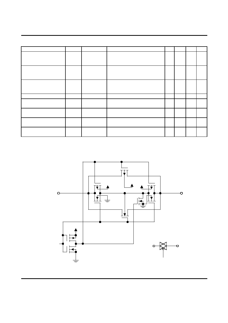
V
DD
V
EE
V
EE
V
DD
V
DD
V
DD
OUT/IN
OUT/IN
IN/OUT
CONTROL
IN/OUT
LEVEL
CONVERTED
CONTROL
Figure 1. Switch Circuit Schematic
UTC 4053 CMOS IC
UTC
UNISONIC TECHNOLOGIES CO., LTD.
5
www.unisonic.com.tw
QW-R502-036,A
TRUTH TABLE
Control Inputs
Select
ON Switches
Inhibit
C B A
UTC 4053
0
0
0
0
0 0 0
0 0 1
0 1 0
0 1 1
Z0 Y0 X0
Z0 Y0 X1
Z0 Y1 X0
Z0 Y1 X1
0
0
0
0
1 0 0
1 0 1
1 1 0
1 1 1
Z1 Y0 X0
Z1 Y0 X1
Z1 Y1 X0
Z1 Y1 X1
1
x x x
None
x = Don't Care
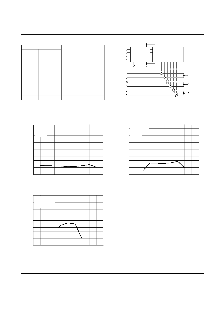
Figure 2. UTC 4053 Functional Diagram
V
EE
V
DD
16
V
SS
8
7
9
B 10
C
A 11
6
INH
LEVEL
CONVERTER
BINARY TO 1 - OF - 2
DECODER WITH
INHIBIT
X0 12
X1 13
Y0 2
Y1 1
Z0 5
Z1 3
14 X
15 Y
4 Z
-10
0
300
350
200
INPUT VOLTAGE, Vin (VOLTS)
250
150
100
50
-8.0 -6.0 -4.0 -2.0 0 2.0 4.0 6.0 8.0 10
-10
0
300
350
200
INPUT VOLTAGE, Vin (VOLTS)
"
O
N
"
R
ESI
ST
AN
C
E
,
R
ON
(O
H
M
S)
250
150
100
50
-8.0 -6.0 -4.0 -2.0
0 2.0 4.0 6.0 8.0 10
"
O
N
"
R
ESI
ST
AN
C
E
,
R
ON
(O
H
M
S)
V
DD
= 7.5 V
V
EE
= - 7.5 V
V
DD
= 5.0 V
V
EE
= -5.0 V
T
a
=25
T
a
=25
-10
0
300
350
200
INPUT VOLTAGE, Vin (VOLTS)
"
O
N
"
R
ESI
ST
A
N
C
E
,
R
ON
(O
H
M
S)
250
150
100
50
-8.0 -6.0 -4.0 -2.0 0
2.0 4.0 6.0 8.0 10
V
DD
= 2.5 V
V
EE
= - 2.5 V
T
a
=25

UTC 4053 CMOS IC
UTC
UNISONIC TECHNOLOGIES CO., LTD.
6
www.unisonic.com.tw
QW-R502-036,A
UTC assumes no responsibility for equipment failures that result from using products at values that
exceed, even momentarily, rated values (such as maximum ratings, operating condition ranges, or
other parameters) listed in products specifications of any and all UTC products described or contained
herein. UTC products are not designed for use in life support appliances, devices or systems where
malfunction of these products can be reasonably expected to result in personal injury. Reproduction in
whole or in part is prohibited without the prior written consent of the copyright owner. The information
presented in this document does not form part of any quotation or contract, is believed to be accurate
and reliable and may be changed without notice.