UTC 75185
LINEAR INTEGRATED CIRCUIT
UTC
UNISONIC TECHNOLOGIES CO., LTD.
1
QW-R113-003,B
MULTIPLE RS-232 DRIVERS AND
RECEIVERS
DESCRIPTION
The UTC 75185 complies with the requirements of the
TIA/EIA232-F and ITU (formerly CCITT) v.28 standards.
These standards are for data interchange between a host
computer and peripheral at signaling rates up to 20kbit/s.
The switching speeds of the UTC 75185 are fast enough
to support rates up to 120kbite/s with lower capacitive
loads (shorter cables). Interoperability at the higher
signaling rates cannot be assured unless the designer
has design control of the cable and the interface circuits
at both ends. For interoperability at signaling rates to
120kbit/s, use of ITA/EIA-423-B (ITU v.10) and
TIA/EIA-422-B (ITU v.11) standards are recommended.
The UTC 75185 is Characterized for operation over
the temperature range of 0
∞C to 70∞C.
FEATURES
*Single chip with easy interface between UART and
Serial-Port connector of IBM
TM
, PC/AT
TM
and
Compatibles.
*Three drivers and five receivers meet or exceed the
requirements of TIA/EIA-232-F and ITU v.28 standards.
*Designed to support data rates up to 120 kbps
*ESD protection meets or exceeds 10 kV on RS-232 pins
and 5 kV on all other pins (Human-Body Model)
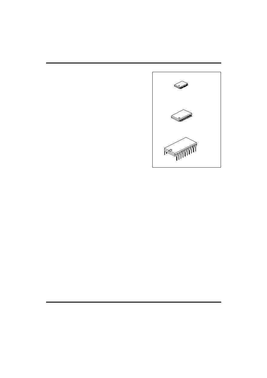
SOP-20
DIP-20
TSSOP-20

UTC 75185
LINEAR INTEGRATED CIRCUIT
UTC
UNISONIC TECHNOLOGIES CO., LTD.
3
QW-R113-003,B
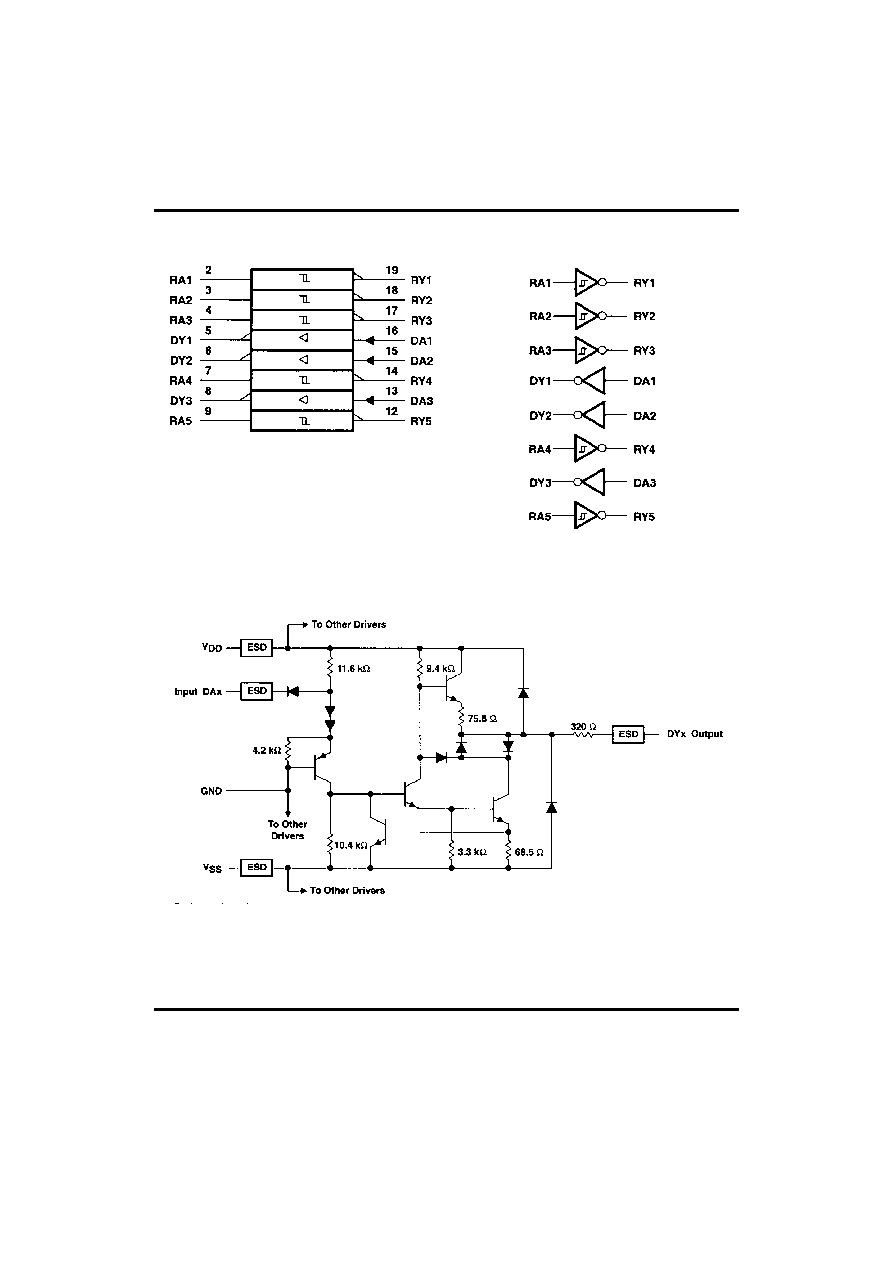
LOGIC SYMBOL AND LOGIC DIAGRAM
This symbol is in accordance with ANSI/IEEE std 91-1984
and IEC Publication 617-12
CIRCUIT OF DRIVERS
(Resistor value shown are nominal.)

UTC 75185
LINEAR INTEGRATED CIRCUIT
UTC
UNISONIC TECHNOLOGIES CO., LTD.
5
QW-R113-003,B
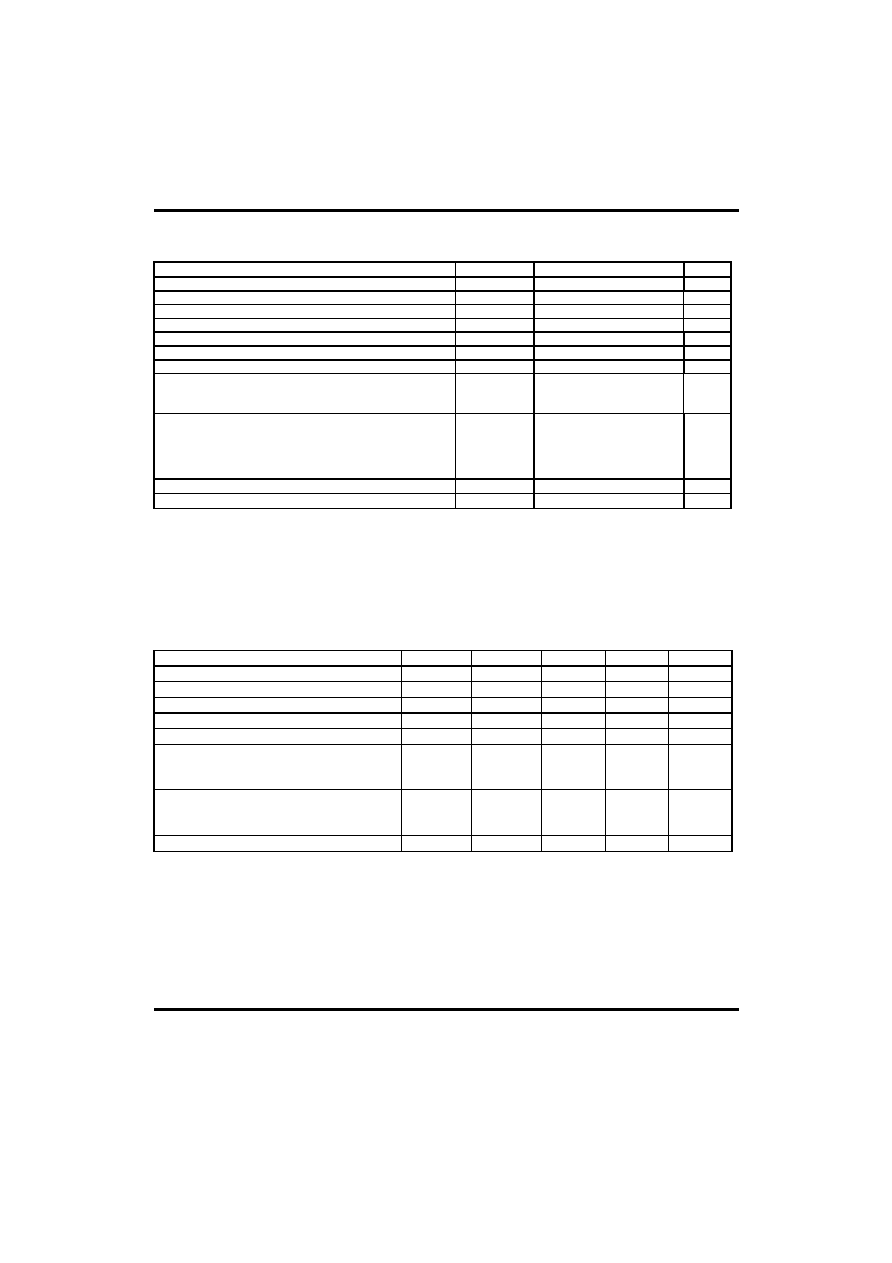
ABSOLUTE MAXIMUM RATINGS OVER OPERATING FREE-AIR TEMPERATURE
RANGE
(unless otherwise specified)
PARAMETER SYMBOL
VALUE
UNIT
Supply voltage (Note 1)
V
DD
15
V
Supply voltage (Note 1)
Vss
-15
V
Supply voltage (Note 1)
Vcc
10
V
Input voltage range (DRIVER)
V
I
-15 to 7
V
Input voltage range (RECEIVER)
V
I
-30 to 30
V
Driver output voltage range
Vo
-15 to 15
V
Receiver low level output current
Io
20
mA
Thermal impedance (note 2)
SOP-20
DIP-20
JA
97
67
∞C/W
Electrostatic discharge
Human-body model: RS-232 pins, class 3, A (note 3)
Human-body model: All pins, class 3, A (note 4)
Machine model: RS-232 pins, class 3, B(note 5)
Machine model: All pins, class 3, B (note 4)
10
5
600
300
kV
kV
V
V
Storage temperature range
Tstg
-65 to +150
∞C
Lead temperature 1.6mm from case for 10 sec
T
L
260
∞C
Note 1: All voltage are with respect to the network ground terminal.
Note 2: The package thermal impedance is calculated in accordance with JESD 51, except for through-hole
packages, which use a trace length of zero.
Note 3: RS-232 pins are tested with respect to ground and each other.
Note 4: Per MIL-PRF-38535.
Note 5: RS-232 pins are tested with respect to ground.
RECOMMENDED OPERATING CONDITIONS
PARAMETER SYMBOL
MIN
TYP
MAX
UNIT
Supply voltage
V
DD
7.5 9 15 V
Supply voltage
V
SS
-7.5 -9 -15 V
Supply voltage
V
CC
4.5 5 5.5 V
High level input voltage (driver only)
V
IH
1.9 V
Low level input voltage (driver only)
V
IL
0.8
V
High level output current
DRIVER
RECEIVER
I
OH
-6.0
-0.5
mA
Low level output current
DRIVER
RECEIVER
I
OL
6
16
mA
Operating free-air temperature
T
A
0 70
∞C
