UTC 75323
LINEAR INTEGRATED CIRCUIT
UTC
UNISONIC TECHNOLOGIES CO., LTD.
1
QW-R113-007,A
MULTIPLE RS-232 DRIVERS AND
RECEIVERS
DESCRIPTION
The UTC 75323 combines five drivers and three
receivers. The flow-through design of the UTC 75323
decreases the part count, reduces the board space
required, and allows easy interconnection of the UART
and serial-port connector. The all-bipolar circuits and
processing of the UTC 75323 provide a rugged,
low-cost solution for this function.
The UTC 75323 complies with the requirements of
the ANSI TIA/EIA-232-Fand ITU (formerly CCITT)
V.28 standards. These standards are for data
interchange between a host computer and a
peripheral at signal rates up to 20 Kbit/s. The
switching speeds of the UTC 75323 are fast enough to
support rates up to 120 kbit/s with lower capacitive
loads (shorter cables). Interoperability at the higher
signaling rates cannot be assured unless the designer
has design control of the cable and the interface
circuits at both ends. For interoperability at signaling
rates up to 120 kbit/s, use of ANSI Standard
TIA/EIA-423-B and TIA/EIA-422-B and
ITU
Recommendations V.10 and V.11 are recommended.
The UTC 75323 is characterized for operation over a
temperature range of 0 to 70.
FEATURES
*Single Chip With Easy Interface Between UART and
Serial-Port Connector of an External Modem or Other
Computer Peripheral
*Five Drivers and Three Receivers Meet or Exceed the
Requirements of ANSI Standard TIA/EIA-232-F and
ITU Recommendation V.28 Standards
.
*Supports Data Rates up to 120 kbit/s.
*Complement to the UTC 75232.
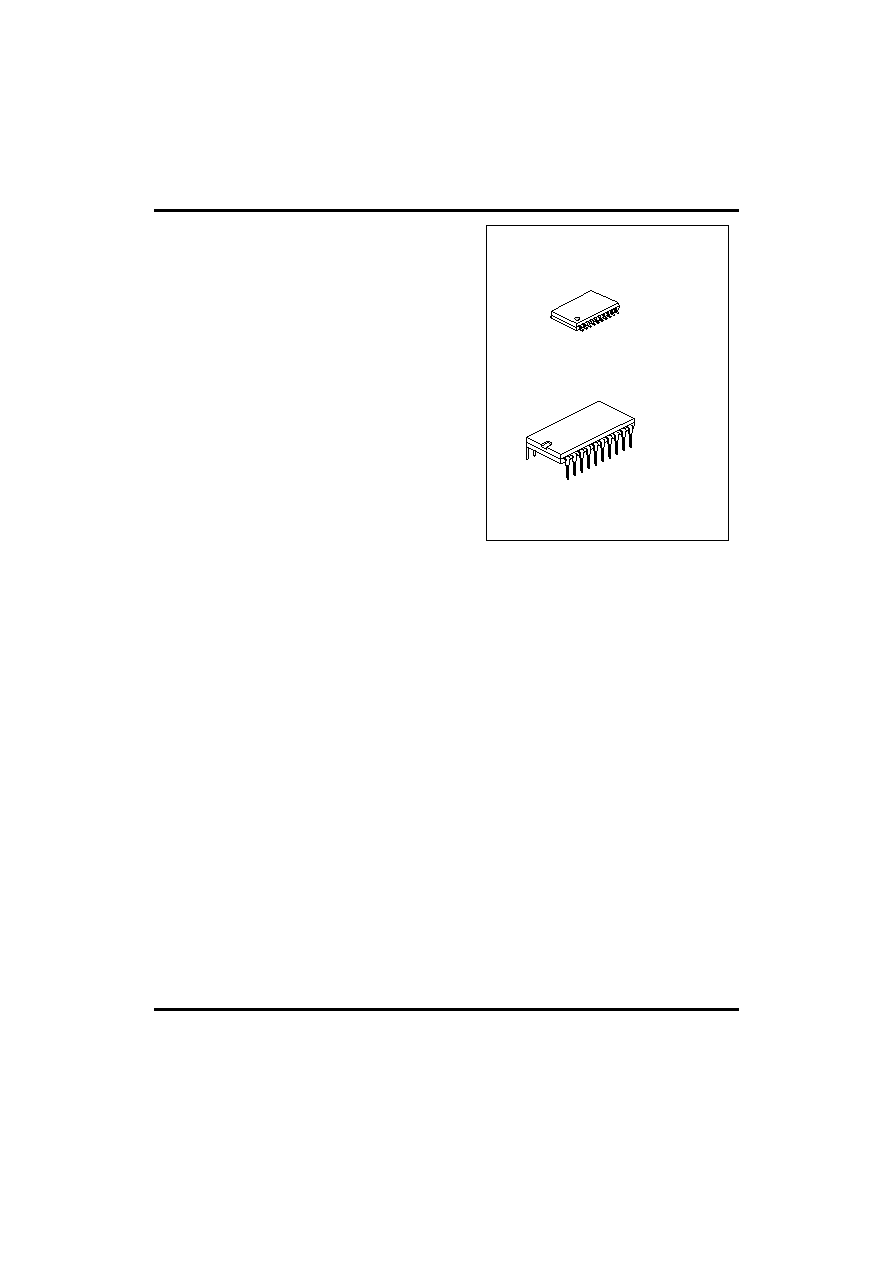
SOP-20
DIP-20
UTC 75323
LINEAR INTEGRATED CIRCUIT
UTC
UNISONIC TECHNOLOGIES CO., LTD.
2
QW-R113-007,A
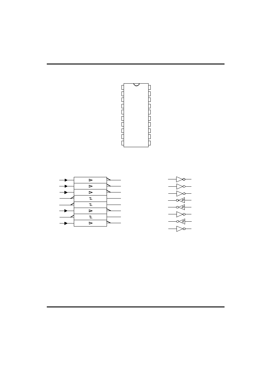
PIN CONFIGURATION
V
DD
1DY
2DY
3DY
1RA
2RA
4DY
3RA
5DY
Vss
GND
5DA
3RY
4DA
2RY
1RY
3DA
2DA
1DA
Vcc
1
2
3
4
5
6
7
8
9
10
11
12
13
14
15
16
17
18
19
20
LOGIC SYMBOL *
2
3
4
5
6
7
8
9
12
13
14
15
16
17
18
19
1DA
2DA
3DA
1RY
2RY
4DA
3RY
5DA
1DY
2DY
3DY
1RA
2RA
4DY
3RA
5DY
* This symbol is in accordance with ANSI/IEEE Std
91-1984 and IEC Publication 617-12.
LOGIC DIAGRAM ( POSITIVE LOGIC )
2
3
4
5
6
7
8
9
12
13
14
15
16
17
18
19
1DA
2DA
3DA
1RY
2RY
4DA
3RY
5DA
1DY
2DY
3DY
1RA
2RA
4DY
3RA
5DY
UTC 75323
LINEAR INTEGRATED CIRCUIT
UTC
UNISONIC TECHNOLOGIES CO., LTD.
3
QW-R113-007,A
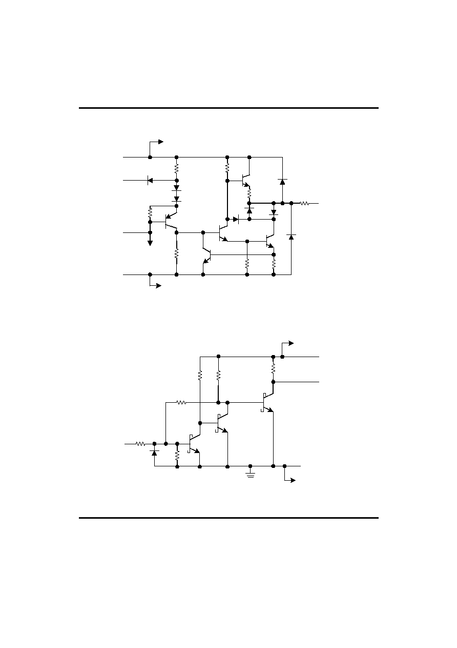
SCHEMATIC (EACH DRIVER)
To Other Drivers
V
DD
Input DAx
GND
Vss
To Other Drivers
To Other
Drivers
10.4k
4.2k
11.6k
9.4k
75.8
320
DYx Output
3.3k
68.5
Resistor values shown are nominal.
SCHEMATIC (EACH RECEIVER)
1.66k
5k
9k
2k
3.8k
10k
GND
To Other Receivers
RYx Output
Vcc
To Other Receivers
Input RAx
Resistor values shown are nominal.
UTC 75323
LINEAR INTEGRATED CIRCUIT
UTC
UNISONIC TECHNOLOGIES CO., LTD.
4
QW-R113-007,A
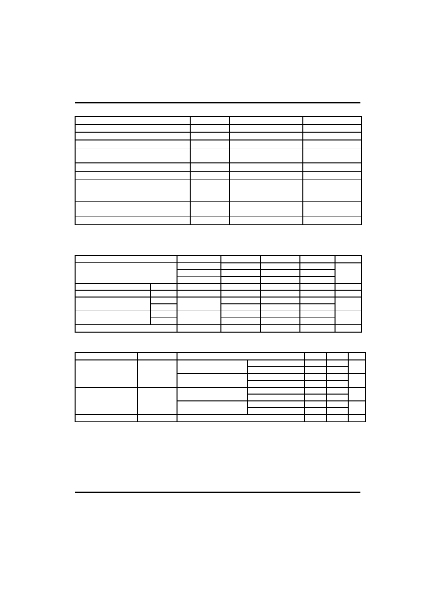
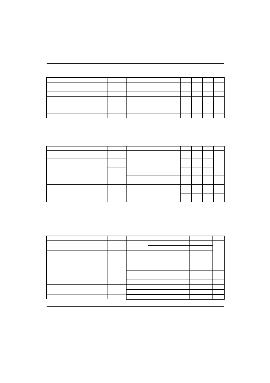
ABSOLUTE MAXIMUM RATINGS
(Ta=25)
PARAMETER SYMBOL
RATINGS UNIT
Supply voltage (see Note 1)
Vcc
10
V
Supply voltage (see Note 1)
V
DD
15
V
Supply voltage (see Note 1)
Vss
-15
V
Input voltage range: Driver
-15 ~ 7
Receiver
V
I
-30 ~ 30
V
Output voltage range, (Driver)
Vo
-15 ~ 15
V
Low-level output current (Receiver)
I
OL
20
mA
Package thermal impedance
SOP-20
DIP-20
JA
97
67
�C/W
Lead temperature 1.6mm(1/6 inch) from case
for 10 seconds
T
lead
260
�C
Storage temperature range
Tstg
-65 ~ 150
�C
note: 1. All voltages are with respect to the network ground terminal.
RECOMMENDED OPERATING CONDITIONS
PARAMETER SYMBOL
MIN
TYP
MAX
UNIT
V
DD
7.5 9 13.5
Vss -7.5 -9
-13.5
Supply voltage
Vcc 4.5 5 5.5
V
High-level input voltage
Driver
V
IH
1.9
V
Low-level input voltage
Driver
V
IL
0.8
V
Driver
-6
High-level output current
Receiver
I
OH
-0.5
mA
Driver
6
High-level output current,
Receiver
I
OL
16
mA
Operating free-air temperature
T
a
0
70
SUPPLY CURRENTS OVER OPERATING FREE-AIR TEMPERATURE RANGE
PARAMETER SYMBOL
TEST
CONDITIONS
MIN
MAX
UNIT
V
DD
=9V, Vss=-9V
25
All inputs at 1.9V, No load
V
DD
=12V, Vss=-12V
32
mA
V
DD
=9V, Vss=-9V
7.5
Supply current from V
DD
I
DD
All inputs at 0.8V, No load
V
DD
=12V, Vss=-12V
9.5
mA
V
DD
=9V, Vss=-9V
-25
All inputs at 1.9V, No load
V
DD
=12V, Vss=-12V
-32
mA
V
DD
=9V, Vss=-9V
-5.3
Supply current from Vss
Iss
All inputs at 0.8V, No load
V
DD
=12V, Vss=-12V
-5.3
mA
Suppy current from Vcc
Icc
Vcc=5V,All inputs at 5V, No load
20
mA
UTC 75323
LINEAR INTEGRATED CIRCUIT
UTC
UNISONIC TECHNOLOGIES CO., LTD.
5
QW-R113-007,A
ELECTRICAL CHARACTERISTICS OVER OPERATING FREE-AIR TEMPERATURE
RANGE,V
DD
=9V,Vss=-9V,Vcc=5V
(UNLESS OTHERWISE NOTED)
PARAMETER
SYMBOL
TEST CONDITIONS
MIN
TYP MAX UNIT
High-level output voltage
V
OH
V
IL
=0.8V,RL=3k (See Figure 1)
6
7.5
V
Low-level output voltage(see Note 2)
V
OL
V
IH
=1.9V,RL=3k (See Figure 1)
-7.5
-6
V
High-level Input current
I
IH
V
I
=5V (See Figure 2)
10
A
Low-level input current
I
IL
V
I
=0 (See Figure 2)
-1.6 mA
High-level short-circuit output current
(see Note 3)
I
OS(H)
V
IL
=0.8V,Vo=0 (See Figure 1)
-4.5
-9 -19.5 mA
Low-level short-circuit output current
I
OS(L)
V
IH
=2V,Vo=0 (See Figure 1)
4.5
9
19
mA
Output resistance (see Note 4)
r
o
Vcc=V
DD
=Vss=0,Vo=-2V to 2V
300
Notes: 2.The algebraic convention, where the more positive(less negative) limit is designated as maximum, is used
in this data sheet for logic levels only,e.g.,if-10V is maximum, the typical value is a more negative voltage.
3.Output short-circuit conditions must maintain the total power dissipation below absolute maximum ratings.
4.Test conditions are those specified by TIA/EIA-232-F and as listed above.
SWITCHING CHARACTERISTICS
(Ta=25,VDD=12V,Vss=-12V,Vcc=5V�10%)
PARAMETER
SYMBOL
TEST CONDITIONS
MIN
TYP MAX UNIT
Propagation delay time, low- to
high-level output
t
PLH
315
500
Propagation delay time, high-to
low-level output
t
PHL
R
L
=3k to 7k, C
L
=15pF
(See Figure 3)
75
175
ns
R
L
=3k to 7k, C
L
=15pF
(See Figure 3)
60
100
ns
TTLH Transition time, low-to high-level
output
t
TLH
R
L
=3k to 7k, C
L
=2500pF
(See Figure 3 and Note 5)
1.7
2.5
s
R
L
=3k to 7k, C
L
=15pF
(See Figure 3)
40 75 ns
Transition time, high-to low-level output
t
THL
R
L
=3k to 7k, C
L
=2500pF
(See Figure 3 and Note 6)
1.5
2.5
s
Note: 5. Measured between-3-V and 3-V points of the output waveform (TIA/EIA-232-F conditions),all unused inputs
are tied either high or low.
6. Measured between 3-V and �3-V points of the output waveform (TIA/EIA-232-F conditions),all unused inputs
are tied either high or low
ELECTRICAL CHARACTERISTICS OVER RECOMMENDED OPERATING
CONDITIONS
(UNLESS OTHERWISE NOTED)
PARAMETER
SYMBOL
TEST CONDITIONS
MIN TYP* MAX UNIT
T
a
=25
1.75
1.9 2.3
Positive-going input threshold voltage
V
IT+
See Figure5
T
a
=0 to 70
1.55
2.3
Negative-going input threshold voltage
V
IT-
0.75
0.97
1.25
Input hysteresis voltage(V
IT
+ - V
IT
-) Vhys
See Figure5
0.5
V
V
IH
=0.75V 2.6
4
5
High-level output voltage
V
OH
I
OH
=-0.5mA
Inputs open
2.6
V
Low-level output voltage
V
OL
I
OL
=10mA,V
I
=3V
0.2
0.45
V
V
I
=25V. 3.6
8.3
dB
High-level input current
I
IH
V
I
=3V 0.43
mA
V
I
=-25V -3.6
-8.3
mA
Low-level input current
I
IL
V
I
=-3V -0.43
mA
Short-circuit output current
Ios
See Figure 4
-3.4
-12
mA
* All typical values are at Ta=25,Vcc=5V,V
DD
=9V,Vss=-9V