 | –≠–ª–µ–∫—Ç—Ä–æ–Ω–Ω—ã–π –∫–æ–º–ø–æ–Ω–µ–Ω—Ç: H654 | –°–∫–∞—á–∞—Ç—å:  PDF PDF  ZIP ZIP |
UNISONIC TECHNOLOGIES CO.,
H654
LINEAR INTEGRATED CIRCUIT
www.unisonic.com.tw
1
Copyright © 2005 Unisonic Technologies Co.,
QW-R118-003,A
COMPLEMENTARY OUTPUT
HALL EFFECT LATCH
DESCRIPTION
The UTC
H654
is integrated Hall sensors with complementary
output drivers designed for electronic commutation of brushless DC
Fan.
It composed of an on-chip Hall voltage generator, a differential
amplifier, Schmitt trigger, an open-collector output on a single chip.
Furthermore, an internal bandgap regulator allows temperature
compensated operations and a wide operating supply range. An
on-chip protection diode is implemented to prevent reverse power
fault.
When the magnetic flux density larger than threshold B
OP
, DO
will be turned on(low) and DOB be turned off(high). The output state
is held until the magnetic flux density is lower than B
RP
, and then DO
is reversal to turned off and DOB turned on.
FEATURES
* Operate from 3.5V ~ 20V supply voltage.
* On-chip Hall sensor with two different sensitivity and hysteresis
settings.
* High output sinking capability up to 300mA for driving large load.
* Lower current change rate reduces the peak output voltages during
switching.
* Build-in protecting diode for chip reversal power connecting.
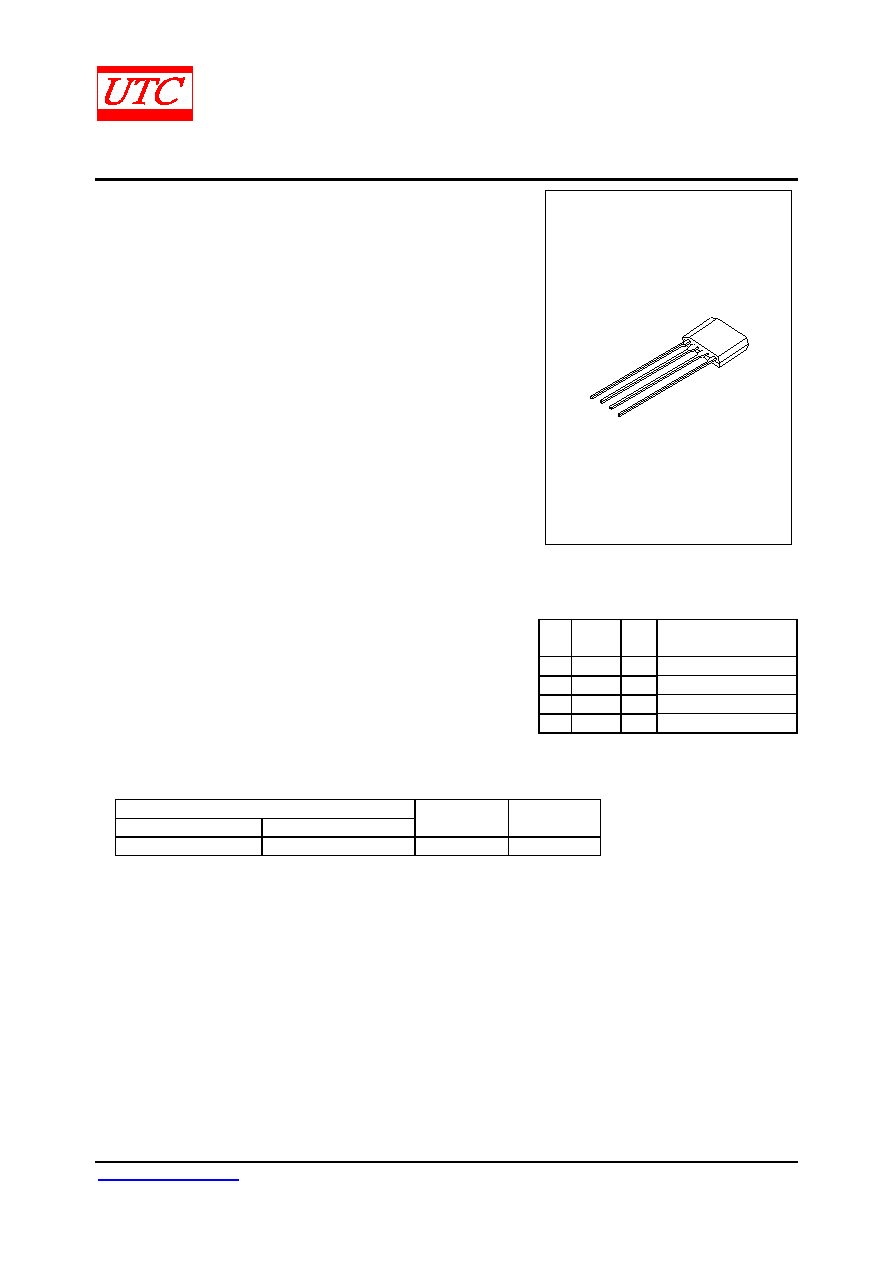
TO-94
1
*Pb-free plating product number: H654L
PIN DESCRIPTION
PIN
NO.
PIN
NAME
P/I/O DESCRIPTION
1
Vcc
P Positive Power Supply
2
DO O
Output
Pin
3
DOB
O Output
Pin
4
Vss
P Ground
ORDERING INFORMATION
Order Number
Normal
Lead free plating
Package Packing
H654-T94-K H654L-T94-K TO-94 Bulk

H654
LINEAR INTEGRATED CIRCUIT
UNISONIC TECHNOLOGIES CO., LTD
2
www.unisonic.com.tw
QW-R118-003,A
BLOCK DIAGRAM
1
V
CC
REG.
Hall
Sensor
DOB
V
SS
DO
1
4
3
2
H654
LINEAR INTEGRATED CIRCUIT
UNISONIC TECHNOLOGIES CO., LTD
3
www.unisonic.com.tw
QW-R118-003,A
ABSOLUTE MAXIMUM RATINGS
(Ta=25)
PARAMETER SYMBOL
RATINGS
UNIT
Supply Voltage
V
CC
20 V
Reverse V
CC
Polarity Voltage
V
RCC
-35 V
Output OFF Voltage
V
CE
50 V
Magnetic flux density
B
Unlimited
Continuous 0.3
Hold 0.4
Output ON Current
Peak (Start Up)
I
C
0.7
A
Power Dissipation
P
D
500
mW
Operating Temperature
T
OPR
0 ~ +70
Junction Temperature
T
J
+125
Storage Temperature
T
STG
-40 ~ +150
Note 1: Output Zener protection voltage
ELECTRICAL CHARACTERISTICS
(Ta =25, unless otherwise specified.)
PARAMETER SYMBOL
TEST
CONDITIONS
MIN
TYP
MAX
UNIT
Low Supply Voltage
V
CE
V
CC
=3.5V, I
L
=100mA
0.4
V
Supply Voltage
V
CC
3.5 20 V
Output Saturation Voltage
V
CE(sat)
V
CC
=14V, I
L
=300mA
0.3
0.6
V
Output Leakage Current
I
CEX
V
CE
=14V, V
CC
=14V
<0.1
10
µA
Supply Current
I
CC
V
CC
=20V, Output Open
16
25
mA
Output Rise Time
t
R
V
CC
=14V, R
L
=820, C
L
=20pF
3.0
10
µS
Output Falling Time
t
F
V
CC
=14V, R
L
=820, C
L
=20pF
0.3
1.5
µS
Switch Time Differential
t V
CC
=14V, R
L
=820, C
L
=20pF
3.0
10
µS
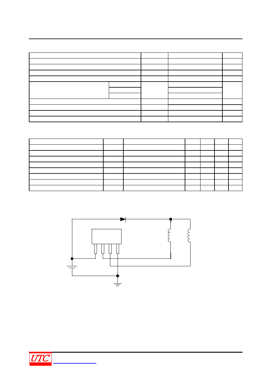
TYPICAL APPLICATION CIRCUIT
1
2 3 4
coil1
coil2
Vcc
+
-
Brushless DC Fan
UTC H654

H654
LINEAR INTEGRATED CIRCUIT
UNISONIC TECHNOLOGIES CO., LTD
4
www.unisonic.com.tw
QW-R118-003,A
TEST CIRCUIT
14V
DOB
R
L1
R
L2
C
L1
C
L2
DO
UTC H654
820
20pF
820
20pF
MAGNETIC CHARACTERISTICS
Ta= 25
Ta= 0 ~ +70
PARAMETR SYMBOL
MIN MAX MIN MAX
UNIT
Operate Point
B
OP
100
100
G
Release Point
B
RP
-100 -100 G
Hysteresis B
HYS
50 200 30 200
G
HYSTERESIS CHARACTERISTICS
100
200
0
-100
-200
ON
RP
OP
OFF
O
u
t
p
u
t
V
o
l
t
a
g
e
in
V
o
l
t
s
Magnetic Flux Density in Gauss
100
200
0
-100
-200
ON
RP
OP
O
u
t
p
u
t
V
o
l
t
a
g
e
i
n
V
o
l
t
s
Magnetic Flux Density in Gauss
OFF
H654
LINEAR INTEGRATED CIRCUIT
UNISONIC TECHNOLOGIES CO., LTD
5
www.unisonic.com.tw
QW-R118-003,A
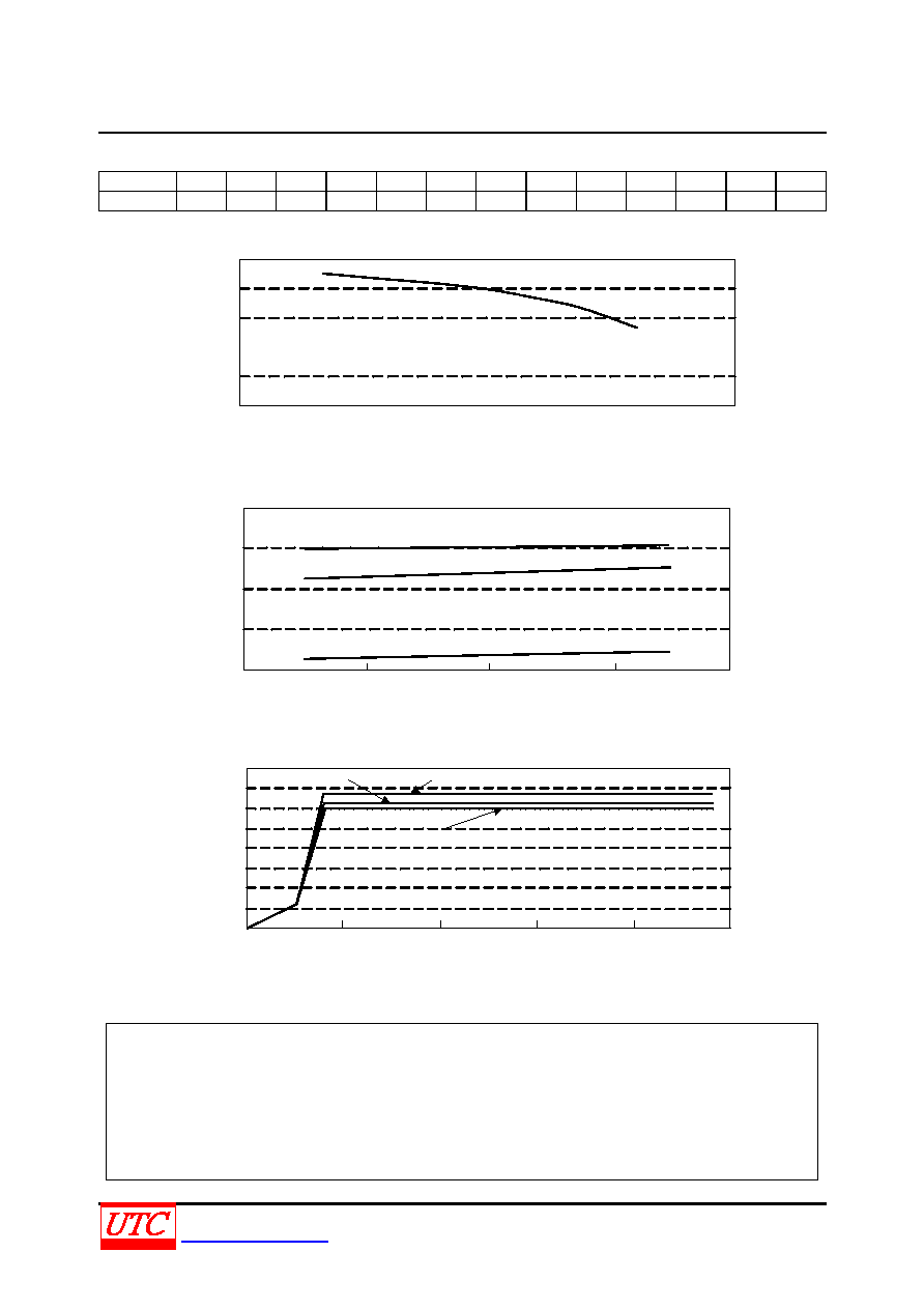
PERFORMANCE CHARACTERISTICS
Ta() 25 50 60 70 80 85 90 95 100
105 110
115 120
P
D
(mW) 550 525 515 505 485
475
465
455
445
425 405 385 365
600
500
400
300
200
100
0
25
50
100
75
150
125
Ta ()
P
D
(m
W
)
Power Dissipation Curve
120
80
0
12
20
B
RP
Supply Voltage (V)
Typical Magnetic Switch Point VS.Supply Voltage
40
-40
5
24
B
OP
B
HYS
F
l
u
x
D
ens
i
t
y
(
G
)
12
4
10
15
Supply Voltage (V)
Typical Supply Current versus Supply Voltage
8
5
20
S
uppl
y
C
u
r
r
ent
(
m
A
)
Ta=25
Ta=80
Ta=20
16
14
10
6
2
0
0
25
UTC assumes no responsibility for equipment failures that result from using products at values that
exceed, even momentarily, rated values (such as maximum ratings, operating condition ranges, or
other parameters) listed in products specifications of any and all UTC products described or contained
herein. UTC products are not designed for use in life support appliances, devices or systems where
malfunction of these products can be reasonably expected to result in personal injury. Reproduction in
whole or in part is prohibited without the prior written consent of the copyright owner. The information
presented in this document does not form part of any quotation or contract, is believed to be accurate
and reliable and may be changed without notice.