 | –≠–ª–µ–∫—Ç—Ä–æ–Ω–Ω—ã–π –∫–æ–º–ø–æ–Ω–µ–Ω—Ç: MCR101-8 | –°–∫–∞—á–∞—Ç—å:  PDF PDF  ZIP ZIP |

UTC MCR101
SCR
UTC
UNISONIC TECHNOLOGIES CO., LTD.
1
QW-R301-009,B
SENSITIVE GATE SILICON
CONTROLLED RECTIFIERS
REVERSE BLOCKING
THYRISTORS
DESCRIPTION
PNPN devices designed for high volume,
line-powered consumer applications such as relay
and lamp drivers, small motor controls, gate drivers
for larger thyristors, and sensing and detection
circuits. Supplied in an inexpensive plastic TO-92
package which is readily adaptable for use in
automatic insertion equipment.
DESCRIPTION
*Sensitive Gate Allows Triggering by Micro controllers
and Other Logic circuits
*Blocking Voltage to 600V
*On-State Current Rating of 0.8A RMS at 80
∞C
*High Surge Current Capability ≠ 10A
*Minimum and Maximum Values of IGT, VGT and IH
Specified for Ease of Design
*Immunity to dV/dt ≠ 20V/
µsec Minimum at 110∞C
*Glass-Passivated Surface for Reliability and
Uniformity
TO-92
1
1: GATE 2: ANODE 3:CATHODE:
THERMAL CHARACTERISTICS
PARAMETER SYMBOL
MAX
UNIT
Thermal Resistance, Junction to Case
R
JC
75
∞C/W
Thermal Resistance, Junction to Ambient
R
JA
200
∞C/W
Lead Solder Temperature
(<1/16" from case, 10 secs max)
T
L
260
∞C
ABSOLUTE MAXIMUM RATINGS
PARAMETER SYMBOL
MAX
UNIT
Peak Repetitive Off-State Voltage(note)
(T
J
=-40 to 110
∞C, Sine Wave, 50 to 60Hz; Gate Open)
MCR101-4
MCR101-6
MCR101-8
V
DRM,
V
RRM
200
400
600
V
On-Sate RMS Current
(Tc=80
∞C) 180∞ Condition Angles
I
T(RMS)
0.8
A
Peak Non-Repetitive Surge Current
(1/2 cycle, Sine Wave, 60Hz, T
J
=25
∞C)
I
TSM
10 A

UTC MCR101
SCR
UTC
UNISONIC TECHNOLOGIES CO., LTD.
2
QW-R301-009,B
PARAMETER SYMBOL
MAX
UNIT
Circuit Fusing Considerations
(t=8.3 ms)
I
2
t 0.415 A
2
s
Forward Peak Gate Power
(T
A
=25
∞C, Pulse Width 1.0µs)
P
GM
0.1 W
Forward Average Gate Power
(T
A
=25
∞C, t=8.3ms)
P
G(AV)
0.1 W
Peak Gate Current ≠ Forward
(T
A
=25
∞C, Pulse Width1.0µs)
I
GM
1 A
Peak Gate Voltage ≠ Reverse
(T
A
=25
∞C, Pulse Width1.0µs)
V
GRM
5 V
Operating Junction Temperature Range @ Rated V
RRM
and
V
DRM
T
J
-40 to +110
∞C
Storage Temperature Range
Tstg
-40 to +150
∞C
Note: V
DRM
and V
RRM
for all types can be applied on a continuous basis. Ratings apply for zero or negative gate
voltage; however, positive gate voltage shall not be applied concurrent with negative potential on the anode.
Blocking voltages shall not be tested with a constant current source such that the voltage ratings of the
devices are exceeded.
ELECTRICAL CHARACTERISTICS
(Tj=25
∞C, unless otherwise stated)
PARAMETER TEST
CONDITION
SYMBOL
MIN
TYP
MAX
UNIT
OFF CHARACTERISTICS
Peak Forward or Reverse Blocking
Current Tc=25
∞C
Tc=125
∞C
V
D
=Rated V
DRM
and V
RRM
; R
GK
=1k
I
DRM
, I
RRM
10
100
µA
µA
ON CHARACTERISTICS
Peak Forward On-State Voltage
(Note1)
I
TM
=1A Peak @ T
A
=25
∞C V
TM
1.7
V
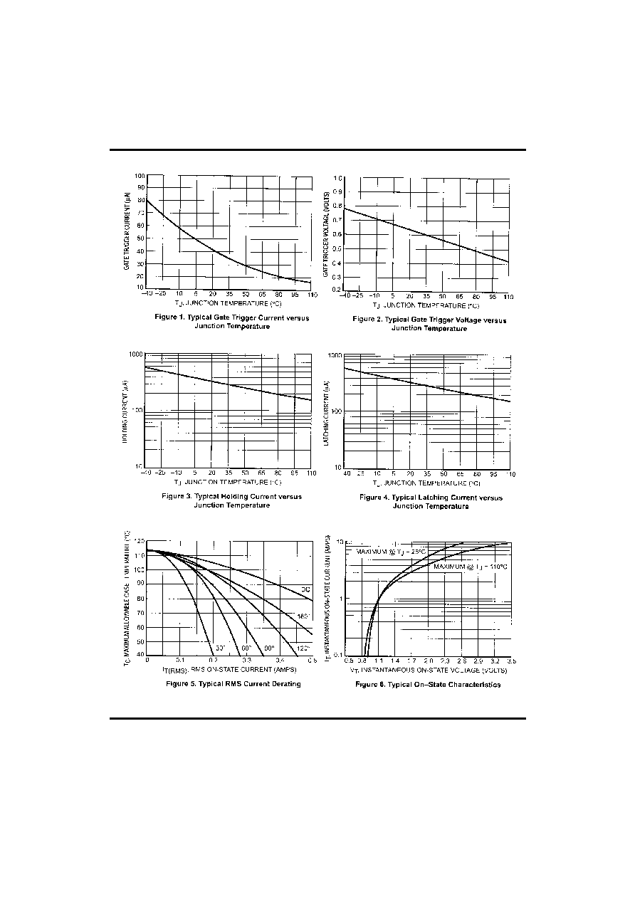
Gate Trigger Current (Continuous
dc)(note2)
V
AK
=7Vdc, R
L
=100
, T
C
=25
∞C I
GT
40
200
µA
Holding Current (note 3) Tc=25
∞C
Tc=-40
∞C
V
AK
=7Vdc, initiating current=20mA
I
H
0.5
5
10
mA
Latch Current Tc=25
∞C
Tc=-40
∞C
V
AK
=7V, Ig=200
µA I
L
0.6
10
15
mA
Gate Trigger Current
(continuous dc) (Note 2) Tc=25
∞C
Tc=-40
∞C
V
AK
=7Vdc, R
L
=100
V
GT
0.62
0.8
1.2
V
DYNAMIC CHARACTERISTICS
Critical Rate of Rise of Off-State
Voltage
V
D
=Rated V
DRM
, Exponential
Waveform, R
GK
=1000
, T
J
=110
∞C
dV/dt 20
35
V/
µs
Critical Rate of Rise of On-State
Current
I
PK
=20A; Pw=10
µsec;
diG/dt=1A/
µsec, Igt=20mA
di/dt
50
A/
µs
Notes: 1. Indicates Pulse Test Width
1.0ms, duty cycle 1%
2. R
GK
=1000
included in measurement.
3. Does not include R
GK
in measurement.
UTC MCR101
SCR
UTC
UNISONIC TECHNOLOGIES CO., LTD.
3
QW-R301-009,B
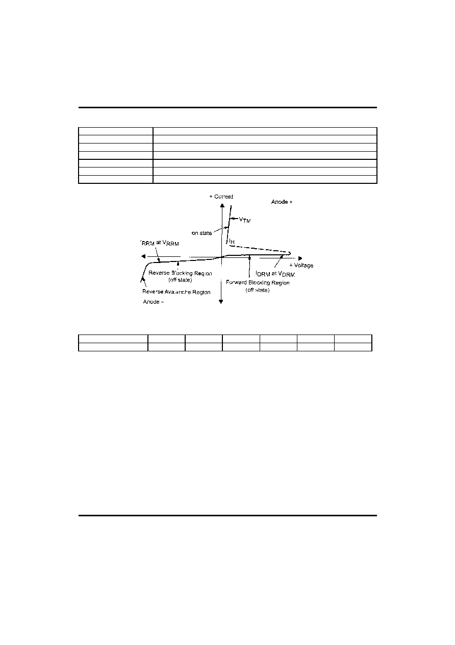
VOLTAGE CURRENT CHARACTERISTIC OF SCR
SYMBOL PARAMETER
V
DRM
Peak Repetitive Off Stat Forward Voltage
I
DRM
Peak Forward Blocking Current
V
RRM
Peak Repetitive Off State Reverse Voltage
I
RRM
Peak Reverse Blocking Current
V
TM
Peak On State Voltage
I
H
Holding
Current
CLASSIFICATION OF I
GT
RANK B
C
AA
AB
AC
AD
RANGE 48~105
µA 95~200µA 8~16µA 14~21µA 19~25µA 23~52µA
UTC MCR101
SCR
UTC
UNISONIC TECHNOLOGIES CO., LTD.
4
QW-R301-009,B