 | –≠–ª–µ–∫—Ç—Ä–æ–Ω–Ω—ã–π –∫–æ–º–ø–æ–Ω–µ–Ω—Ç: UR233 | –°–∫–∞—á–∞—Ç—å:  PDF PDF  ZIP ZIP |
UTC UR233
LINEAR INTEGRATED CIRCUIT
UTC
UNISONIC TECHNOLOGIES CO., LTD.
1
QW-R102-011,C
LOW DROP FIXED AND
ADJUSTABLE POSITIVE VOLTAGE
REGULATORS
DESCRIPTION
The UTC UR233 is a LOW DROP Voltage Regulator able
to provide up to 0.8A of Output Current, available even in
adjustable version (Vref=1.25V). Concerning fixed versions,
are offered the following Output Voltages: 1.8V, 2.5V, 2.85V,
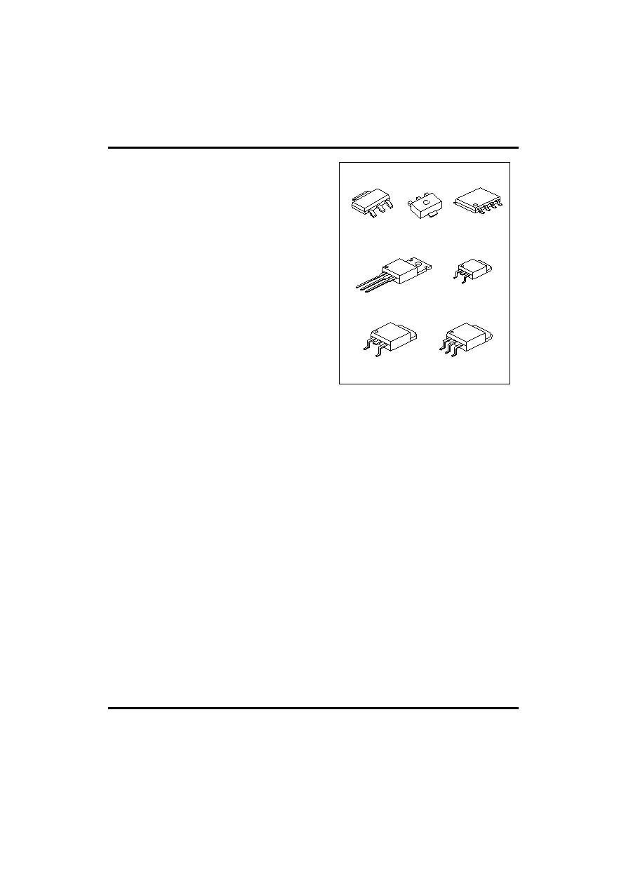
3.0V, 3.3V and 5.0V. The device is supplied in: SOT-223,
SOT-89,TO-252, TO-263, TO-263-3, SOP-8 and TO-220. The
SOT-223,SOT-89,SOP-8,TO-263,TO-263-3 and TO-252
surface mount packages optimize the thermal characteristics
even offering a relevant space saving effect. High efficiency is
assured by NPN pass transistor. In fact in the case, unlike
than PNP one, the Quiescent Current flows mostly into the
load. Only a very common 10
µ
F minimum capacitor is needed
for stability. On chip trimming allows the regulator to reach a
very tight output voltage tolerance, within
±
1% at 25
∞
C. The
ADJUSTABLE UR233 is pin to pin compatible with the other
standard Adjustable voltage regulators maintaining the better
performances in terms of Drop and Tolerance.
FEATURES
*Low dropout voltage (1V Typ.)
*Output current up to 0.8A
*Fixed output voltage of: 1.8V,2.5V, 2,85V, 3.0V, 3.3V, 5.0V
*Adjustable version availability (Vref=1.25V)
*Internal current and thermal limit
*Available in
±
1%(at 25
∞
C) and 2% in all temperature range
*Supply voltage rejection: 75dB (TYP)
*Temperature range: 0
∞
C to 125
∞
C
SOP-8
SOT-223
1
TO-220
TO-252
TO-263
1
1
1
TO-263-3
1
1
SOT-89
SOP-8 1: GND; 2,3,6,7: Vout;
4: Vin; 5,8: NC
*Pb-free plating product number: UR233L
UTC UR233
LINEAR INTEGRATED CIRCUIT
UTC
UNISONIC TECHNOLOGIES CO., LTD.
2
QW-R102-011,C
MARKING INFORMATION
PACKAGE VOLTAGE
CODE
PIN CODE PIN 1
PIN 2
PIN 3
MARKING
A GND
OUT
IN
B OUT
GND
IN
C GND
IN
OUT
SOT-223
D IN
GND
OUT
1
2
3
UR233
VOLTAGE
CODE
DATE
CODE
PIN CODE
A GND
OUT
IN
B OUT
GND
IN
C GND
IN
OUT
SOT-89
D IN
GND
OUT
1
2
3
UR233
DATE
CODE
PIN CODE
VOLTAGE
CODE
A GND
OUT
IN
B OUT
GND
IN
C GND
IN
OUT
TO-220
TO-252
TO-263
TO-263-3
1 8 : 1 . 8 V
2 5 : 2 . 5 V
2 8 : 2 . 8 5 V
3 0 : 3 . 0 V
3 3 : 3 . 3 V
5 0 : 5 . 0 V
A D : A D J
D IN
GND
OUT
1
2
3
UTC
UR233
VOLTAGE
CODE
DATE
CODE
PIN CODE
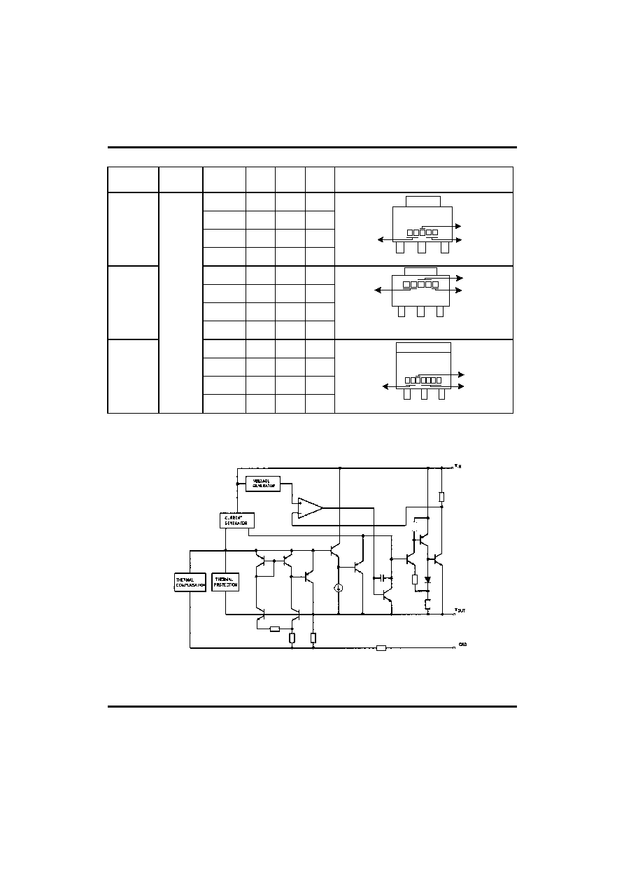
BLOCK DIAGRAM

UTC UR233
LINEAR INTEGRATED CIRCUIT
UTC
UNISONIC TECHNOLOGIES CO., LTD.
3
QW-R102-011,C
ABSOLUTE MAXIMUM RATINGS
PARAMETER SYMBOL
VALUE
UNIT
DC Input Voltage
V
IN
12 V
Power Dissipation
Ptot
12
W
Storage temperature
Tstg
-65 ~ +150
∞
C
Operating Junction
Temperature
Top
0 ~ +125
∞
C
Note: Absolute Maximum Ratings are those value beyond which damage to the device may occur. Functional
operation under there condition is not implied. Over the above suggested Max Power Dissipation a Short Circuit
could definitively damage the device.
THERMAL DATA
PARAMETER SYMBOL
VALUE
UNIT
Thermal Resistance Junction-case
SOT-223
SOP-8
TO-252
TO-220
TO-263
Rth-case
15
20
8
3
3
∞
C/W
∞
C/W
∞
C/W
∞
C/W
∞
C/W
Thermal Resistance Junction-ambient
TO-220
Rthj-amb
50
∞
C/W
UTC UR233-1.8 ELECTRICAL CHARACTERISTICS
(refer to the test circuits, Tj=0 to 125
∞
C, Co=10
µ
F unless otherwise specified)
PARAMETER
SYMBOL TEST
CONDITIONS MIN.
TYP.
MAX.
UNIT
Output Voltage
Vo
Vin=3.8V, Io=10mA, Tj=25
∞
C 1.782
1.800
1.818
V
Output Voltage
Vo
Io=2 to 800mA, Vin=3.2 to 10V
1.764
1.836
V
Line Regulation
Vo
Vin=3.2 to 10V, Io=2mA
1
6
mV
Load Regulation
Vo
Vin=3.2V, Io=2 to 800/mA
1
10
mV
Temperature stability
Vo
0.5
%
Long Term Stability
Vo
1000 hrs, Tj=125
∞
C
0.3
%
Operating Input Voltage
Vin
Io=100mA
12
V
Quiescent Current
Id
Vin
10V
5
10
mA
Output Current
Io
Vin=6.8V, Tj=25
∞
C 800
950
1200
mA
Output Noise Voltage
eN
B=10Hz to 10KHz, Tj=25
∞
C
100
µ
V
Supply Voltage
Rejection
SVR
Io=40mA, f=120Hz, Tj=25
∞
C, Vin=4.8V,
Vripple=1Vpp
60
75 dB
Dropout Voltage
Vd
1.50
V
Thermal Regulation
Ta=25
∞
C, 30ms Pulse
0.01
0.10
%/W
UTC UR233 ELECTRICAL CHARACTERISTICS
(refer to the test circuits, Tj=0 to 125
∞
C, Co=10
µ
F unless otherwise specified)
PARAMETER
SYMBOL TEST
CONDITIONS MIN.
TYP.
MAX.
UNIT
Output Voltage
Vo
Vin=4.5V, Io=10mA, Tj=25
∞
C
±
1%
±2
%
2.475
2.450
2.500
2.500
2.525
2.550
V
V
Output Voltage
Vo
Io=2 to 800mA,
±2
%
Vin=3.9 to 10V
±4
%
2.450
2.400
2.550
2.600
V
V
Line Regulation
Vo
Vin=3.9 to 10V, Io=2mA
1
6
mV
Load Regulation
Vo
Vin=3.9V, Io=2 to 800mA
1
10
mV
Temperature stability
Vo
0.5
%
UTC UR233
LINEAR INTEGRATED CIRCUIT
UTC
UNISONIC TECHNOLOGIES CO., LTD.
4
QW-R102-011,C
PARAMETER
SYMBOL TEST
CONDITIONS MIN.
TYP.
MAX.
UNIT
Long Term Stability
Vo
1000 hrs, Tj=125
∞
C
0.3
%
Operating Input Voltage
Vin
Io=100mA
12
V
Quiescent Current
Id
Vin
10V
5
10
mA
Output Current
Io
Vin=7.5V, Tj=25
∞
C 800
950
1200
mA
Output Noise Voltage
eN
B=10Hz to 10KHz, Tj=25
∞
C
100
µ
V
Supply Voltage
Rejection
SVR
Io=40mA, f=120Hz, Tj=25
∞
C, Vin=5.5V,
Vripple=1Vpp
60
75 dB
Dropout Voltage
Vd
1.50
V
Thermal Regulation
Ta=25
∞
C, 30ms Pulse
0.01
0.10
%/W
UTC UR233-2.85 ELECTRICAL CHARACTERISTICS
(refer to the test circuits, Tj=0 to 125
∞
C, Co=10
µ
F unless otherwise specified)
PARAMETER
SYMBOL TEST
CONDITIONS MIN.
TYP.
MAX.
UNIT
Output Voltage
Vo
Vin=4.85V, Io=10mA, Tj=25
∞
C 2.82
2.85
2.88
V
Output Voltage
Vo
Io=2 to 800mA,Vin=4.25 to 10V
2.79
2.91
V
Line Regulation
Vo
Vin=4.25 to 10V, Io=2mA
1
6
mV
Load Regulation
Vo
Vin=4.25V, Io=2 to 800mA
1
10
mV
Temperature stability
Vo
0.5
%
Long Term Stability
Vo
1000 hrs, Tj=125
∞
C
0.3
%
Operating Input Voltage
Vin
Io=100mA
12
V
Quiescent Current
Id
Vin
10V
5
10
mA
Output Current
Io
Vin=7.85V, Tj=25
∞
C 800
950
1200
mA
Output Noise Voltage
eN
B=10Hz to 10KHz, Tj=25
∞
C
100
µ
V
Supply Voltage
Rejection
SVR
Io=40mA, f=120Hz, Tj=25
∞
C, Vin=5.85V,
Vripple=1Vpp
60
75 DB
Dropout Voltage
Vd
1.50
V
Thermal Regulation
Ta=25
∞
C, 30ms Pulse
0.01
0.10
%/W
UTC UR233-3.0 ELECTRICAL CHARACTERISTICS
(refer to the test circuits, Tj=0 to 125
∞
C, Co=10
µ
F unless otherwise specified)
PARAMETER
SYMBOL TEST
CONDITIONS MIN.
TYP.
MAX.
UNIT
Output Voltage
Vo
Vin=5V, Io=10mA, Tj=25
∞
C
±
1%
±2
%
2.97
2.94
3.00
3.00
3.03
3.06
V
V
Output Voltage
Vo
Io=2 to 800 mA
±2
%
Vin=4.5 to 10V
±4
%
2.94
2.88
3.06
3.12
V
V
Line Regulation
Vo
Vin=4.5 to 12V, Io=2mA
1
6
mV
Load Regulation
Vo
Vin=4.5V, Io=2 to 800mA
1
10
mV
Temperature stability
Vo
0.5
%
Long Term Stability
Vo
1000 hrs, Tj=125
∞
C
0.3
%
Operating Input Voltage
Vin
Io=100mA
12
V
Quiescent Current
Id
Vin
12V
5
10
mA
Output Current
Io
Vin=8V, Tj=25
∞
C 800
950
1200
mA
Output Noise Voltage
eN
B=10Hz to 10KHz, Tj=25
∞
C
100
µ
V
Supply Voltage
Rejection
SVR
Io=40mA, f=120Hz, Tj=25
∞
C, Vin=6V,
Vripple=1Vpp
60
75 dB
Dropout Voltage
Vd
1.50
V
Thermal Regulation
Ta=25
∞
C, 30ms Pulse
0.01
0.10
%/W
UTC UR233
LINEAR INTEGRATED CIRCUIT
UTC
UNISONIC TECHNOLOGIES CO., LTD.
5
QW-R102-011,C
UTC UR233-3.3 ELECTRICAL CHARACTERISTICS
(refer to the test circuits, Tj=0 to 125
∞
C, Co=10
µ
F unless otherwise specified)
PARAMETER
SYMBOL TEST
CONDITIONS MIN.
TYP.
MAX.
UNIT
Output Voltage
Vo
Vin=5.3V, Io=10mA, Tj=25
∞
C
±
1%
±2
%
3.267
3.235
3.300
3.300
3.333
3.365
V
V
Output Voltage
Vo
Io=2 to 800mA,
±2
%
Vin=4.75 to 10V
±4
%
3.235
3.160
3.365
3.440
V
V
Line Regulation
Vo
Vin=4.75 to 12V, Io=2mA
1
6
mV
Load Regulation
Vo
Vin=4.75V, Io=2 to 800mA
1
10
mV
Temperature stability
Vo
0.5
%
Long Term Stability
Vo
1000 hrs, Tj=125
∞
C
0.3
%
Operating Input Voltage
Vin
Io=100mA
12
V
Quiescent Current
Id
Vin
12V
5
10
mA
Output Current
Io
Vin=8.3V, Tj=25
∞
C 800
950
1200
mA
Output Noise Voltage
eN
B=10Hz to 10KHz, Tj=25
∞
C
100
µ
V
Supply Voltage
Rejection
SVR
Io=40mA, f=120Hz, Tj=25
∞
C, Vin=6.3V,
Vripple=1Vpp
60
75 DB
Dropout Voltage
Vd
1.50
V
Thermal Regulation
Ta=25
∞
C, 30ms Pulse
0.01
0.10
%/W
UTC UR233-5.0 ELECTRICAL CHARACTERISTICS
(refer to the test circuits, Tj=0 to 125
∞
C, Co=10
µ
F unless otherwise specified)
PARAMETER
SYMBOL TEST
CONDITIONS MIN.
TYP.
MAX.
UNIT
Output Voltage
Vo
Vin=7V, Io=10mA, Tj=25
∞
C
±
1%
±2
%
4.95
4.90
5.00
5.00
5.05
5.10
V
V
Output Voltage
Vo
Io=2 to 800mA,
±2
%
Vin=6.5 to 12V
±4
%
4.90
4.80
5.10
5.20
V
V
Line Regulation
Vo
Vin=6.5 to 12V, Io=2mA
1
10
mV
Load Regulation
Vo
Vin=6.5V, Io=2 to 800mA
1
15
mV
Temperature stability
Vo
0.5
%
Long Term Stability
Vo
1000 hrs, Tj=125
∞
C
0.3
%
Operating Input Voltage
Vin
Io=100mA
12
V
Quiescent Current
Id
Vin
12V
5
10
mA
Output Current
Io
Vin=10V, Tj=25
∞
C 800
950
1200
mA
Output Noise Voltage
eN
B=10Hz to 10KHz, Tj=25
∞
C
100
µ
V
Supply Voltage
Rejection
SVR
Io=40mA, f=120Hz, Tj=25
∞
C, Vin=8V,
Vripple=1Vpp
60
75 dB
Dropout Voltage
Vd
1.50
V
Thermal Regulation
Ta=25
∞
C, 30ms Pulse
0.01
0.10
%/W