UNISONIC TECHNOLOGIES CO.,LTD
UR5596
MOS IC
www.unisonic.com.tw
1
Copyright © 2005 Unisonic Technologies Co.,LTD
QW-R502-045,A
DDR TERMINATION
REGULATOR
DESCRIPTION
The UTC
UR5596
is a linear bus termination regulator and
designed to meet JEDEC SSTL-2(Stub-Series Terminated
Logic) specifications for termination of DDR-SDRAM. It also can
be used in SSTL-3 or HSTL(High-Speed Transceiver Logic)
scheme. The device contains a high-speed OP AMP to provide
excellent response to the load transients, and can deliver 1.5A
continuous current and transient peaks up to 3A in the
application as required for DDR-SDRAM termination.
The UTC
UR5596
also incorporates a V
SENSE
pin to provide
superior load regulation and a V
REF
output as a reference for the
chipset and DIMMs. Besides, an active low shutdown (SHDN)
pin provides Suspend To RAM (STR) functionality. When SHDN
is pulled low the V
TT
output will tri-state providing a high
impedance output, but, V
REF
will remain active. A power savings
advantage can be obtained in this mode through lower
quiescent current.
Regarding the output, V
TT
is capable of sinking and sourcing
current while regulating the output voltage equal to V
DDQ
/2. The
output stage has been designed to maintain excellent load
regulation while preventing shoot through. The UTC
UR5596
also incorporates two distinct power rails that separates the
analog circuitry from the power output stage. This allows a split
rail approach to be utilized to decrease internal power
dissipation and permits UTC
UR5596
to provide a termination
solution for DDRII SDRAM.
FEATURES
* Source and sink current
* Low output voltage offset
* No external resistors required
* Linear topology
* Suspend To Ram (STR) functionality
* Low external component count
* Thermal shutdown protection
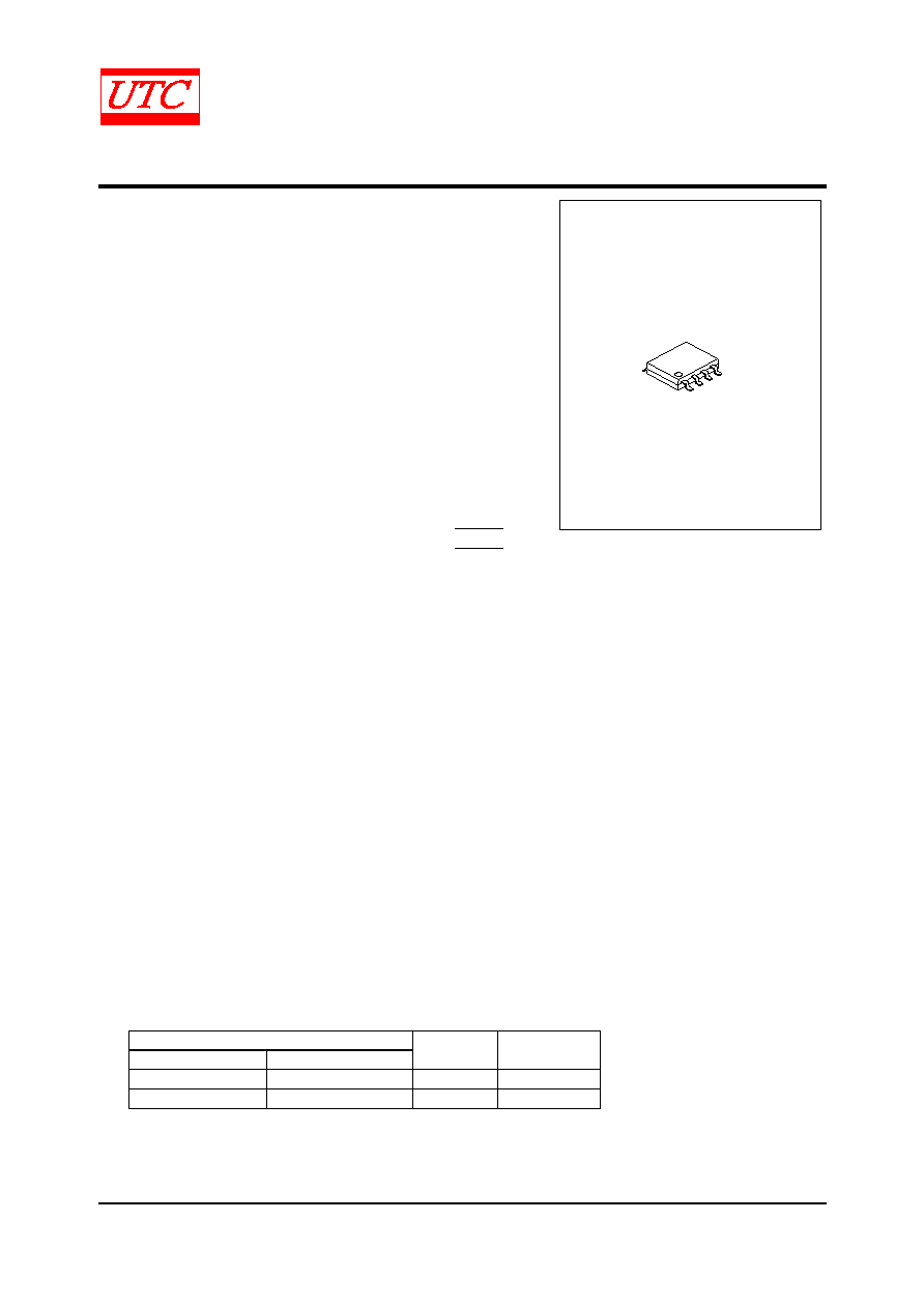
SOP-8
*Pb-free plating product number: UR5596L
ORDERING INFORMATION
Ordering Number
Normal
Lead Free Plating
Package
Packing
UR5596-S08-R UR5596L-S08-R SOP-8 Tape
Reel
UR5596-S08-T UR5596L-S08-T SOP-8
Tube

UR5596
MOS IC
UNISONIC TECHNOLOGIES CO., LTD
2
www.unisonic.com.tw
QW-R502-045,A
PIN CONFIGURATION
4
3
2
1
5
6
7
8
V
TT
AV
IN
PV
IN
V
DDQ
V
SENSE
V
REF
GND
SHDN
PIN DESCRIPTION
PIN NO.
PIN NAME
PIN FUNCTION
1 GND
Ground
2 SHDN
Shutdown
3 V
SENSE
Feedback pin for regulating V
TT
.
4 V
REF
Buffered internal reference voltage of V
DDQ
/2
5 V
DDQ
Input for internal reference equal to V
DDQ
/2
6 AV
IN
Analog input pin
7 PV
IN
Power input pin
8 V
TT
Output voltage for connection to termination resistors
BLOCK DIAGRAM
-
+
-
+
50k
50k
V
DDQ
AV
IN
PV
IN
V
TT
V
SENSE
GND
V
REF
SHDN

UR5596
MOS IC
UNISONIC TECHNOLOGIES CO., LTD
3
www.unisonic.com.tw
QW-R502-045,A
ABSOLUTE MAXIMUM RATINGS
PARAMETER SYMBOL
RATINGS
UNIT
PV
IN
, AV
IN
, V
DDQ
to GND
V
DD
-0.3 ~ +6
V
Supply Voltage
AV
IN
to GND(Note 1)
V
DD
2.2 ~ 5.5
V
Junction Temperature
T
J
125
Operation Temperature(Note 2)
T
OPR
-20 ~ +85
Storage Temperature
T
STG
-40 ~ +150
Thermal Resistance Junction-Ambient
JA
150
/W
Note: 1.Signified recommend operating range that indicates conditions for which the device is intended to be
functional, but does not guarantee specific performance limits.
2.The device is guaranteed to meet performance specification within 0~70 operating temperature range
and assured by design from ≠20~+85.
3.Absolute maximum ratings indicate limits beyond which damage to the device may occur.
ELECTRICAL CHARACTERISTICS
(T
J
=25∞C, V
IN
=AV
IN
=PV
IN
=2.5V, V
DDQ
=2.5V, unless otherwise specified).
PARAMETER SYMBOL
TEST
CONDITIONS
MIN
TYP
MAX
UNIT
V
REF
Voltage
V
REF
V
IN
= V
DDQ
= 2.3V
V
IN
= V
DDQ
= 2.5V
V
IN
= V
DDQ
= 2.7V
1.135
1.235
1.335
1.158
1.258
1.358
1.185
1.285
1.385
V
I
OUT
= 0A
V
IN
= V
DDQ
= 2.3V
V
IN
= V
DDQ
= 2.5V
V
IN
= V
DDQ
= 2.7V
1.125
1.225
1.325
1.159
1.259
1.359
1.190
1.290
1.390
V
TT
Output Voltage
I
OUT
= ±1.5A
V
TT
V
IN
= V
DDQ
= 2.3V
V
IN
= V
DDQ
= 2.5V
V
IN
= V
DDQ
= 2.7V
1.125
1.225
1.325
1.159
1.259
1.359
1.190
1.290
1.390
V
High V
IH
1.9
Minimum Shutdown Level
Low V
IL
0.8
V
V
TT
Output Voltage Offset (V
REF
- V
TT
)
Vos
TT
V
TT
I
OUT
= 0A
I
OUT
= -1.5A
I
OUT
= +1.5A
-20
-25
-25
0
0
0
20
25
25
mV
Quiescent Current
I
Q
I
OUT
= 0A
320
500
µA
Quiescent Current in Shutdown
I
SD
SD = 0V
115
150
µA
Shutdown Leakage Current
I
Q_SD
SD = 0V
2
5
µA
V
TT
Leakage Current in Shutdown
I
V
SD = 0V
V
TT
= 1.25V
1
10
µA
V
SENSE
Input Current
I
SENSE
13
nA
V
REF
Output Impedance
Z
VREF
I
REF
= -30 ~ +30 µA
2.5
k
V
DDQ
Input Impedance
Z
VDDQ
100
k
Thermal Shutdown
T
SD
165
Thermal Shutdown Hysteresis
T
SD-HYS
10

UR5596
MOS IC
UNISONIC TECHNOLOGIES CO., LTD
4
www.unisonic.com.tw
QW-R502-045,A
PIN DESCRIPTIONS
AV
IN
, PV
IN
Input supply pins
. AV
IN
is used to supply all the internal analog circuits and PV
IN
is used to provide the output stage
to create V
TT
. These pins have the capability to work off separate supplies depending on the application. Higher
voltages on PV
IN
will increase the maximum continuous output current because of output RDSON limitations at
voltages close to V
TT
. But the internal power loss will also increase, thermally limiting the design. If the junction
temperature exceeds the thermal shutdown than the part will enter a shutdown state identical to the manual
shutdown where V
TT
is tri-stated and V
REF
remains active.
For SSTL-2 applications, a good compromise would be to connect the AV
IN
and PV
IN
directly together at 2.5V. This
eliminates the need for bypassing the two supply pins separately. The only limitation on input voltage selection is
that PV
IN
must be equal to or lower than AV
IN
. It is recommended to connect PV
IN
to voltage rails equal to or less
than 3.3V to prevent the thermal limit from tripping because of excessive internal power dissipation.
V
DDQ
The input pin used to create the internal reference voltage from a resistor divider of two internal 50k resistors for
regulating V
TT
and to guarantee V
TT
will track V
DDQ
/2 precisely. As a remote sense by connecting V
DDQ
directly to the
2.5V rail for SSTL-2 applications is an optimal implementation of V
DDQ
at the DIMM. This ensures that the reference
voltage tracks the DDR memory rails precisely without a large voltage drop from the power lines.
V
SENSE
The sense pin supply improved remote load regulation, if remote load regulation is not used then the V
SENSE
pin
must still be connected to V
TT
. A long trace will cause a significant IR drop resulting in a termination voltage lower at
one end of the bus than the other. Connect V
SENSE
pin to the middle of the bus to provide a better distribution across
the entire termination bus then DDR performance will be improved. Take notice of when a long V
SENSE
trace is
implemented in close proximity to the memory, noise pickup in the V
SENSE
trace can cause problems with precise
regulation of V
TT
. A ceramic capacitor of 0.1uF is placed to next the V
SENSE
pin can help filter any high frequency
signals and preventing errors.
V
REF
V
REF
supply the buffered output of the internal reference voltage V
DDQ
/2. This output delivers the reference voltage
for the Northbridge chipset and memory. Since these inputs are typically extremely high impedance, there should be
little current drawn from V
REF
. A 0.1µF~0.01µF ceramic capacitor could be used to acquire better performance,
located close to the pin to help with noise. This output remains active during the shutdown state and thermal
shutdown events for the suspend to RAM functionality.
V
TT
V
TT
is a regulated output for the bus resistors termination of DDR-SDRAM. It can track precisely the V
DDQ
/2
voltage with the sinking and sourcing current capability. The UTC
UR5596
is designed to handle peak transient
currents of up to ± 3A with a fast transient response. If a transient is expected to remain above the maximum
continuous current rating for a significant amount of time then the output capacitor size should be large enough to
prevent an excessive voltage drop.
Although UTC
UR5596
can handle large transient output currents, but it can not handling these for long durations
since the limited thermal dissipation capability of SOP-8 package. If large currents are required for longer durations,
then must ensure the maximum junction temperature is not exceeded, otherwise, the maximum output current will be
degraded with heating. Proper thermal de-rating should always be used. While the temperature beyond the junction
temperature, the thermal shutdown protection will be functioned, then V
TT
will tri-state until the part returns below the
hysteretic trigger point.

UR5596
MOS IC
UNISONIC TECHNOLOGIES CO., LTD
5
www.unisonic.com.tw
QW-R502-045,A
CAPACITOR SELECTION
A capacitor is recommended for improve performance during large load transients to prevent the input rail from
dropping, even though
UR5596
does not require for input stability. The input capacitor should be located as close as
possible to the PV
IN
pin. The typical recommended value for AL electrolytic capacitors is 50 µF and 10 µF with X5R
or better for Ceramic capacitors. If AV
IN
and PV
IN
are separated, the 47µF capacitor should be placed as close to
possible to the PV
IN
rail. An additional 0.1uF ceramic capacitor can be placed on the AVIN rail to prevent excessive
noise from coupling into the device.
UTC
UR5596
has been designed to be insensitive of output capacitor size or ESR (Equivalent Series Resistance).
The choice for output capacitor depends on the application and the requirements for load transient response of V
TT
.
As a general recommendation the output capacitor should be sized above 100 µF with a low ESR for SSTL
applications with DDR-SDRAM. The value of ESR should be determined by the maximum current spikes expected
and the extent at which the output voltage is allowed to droop.
THERMAL DISSIPATION
The UR5596 will generate heat result from internal power dissipation when current flow working. The device might
be damaged any beyond maximum junction temperature rating. The maximum allowable internal temperature rise
(T
Rmax
) can be calculated given the maximum ambient temperature (T
Amax
) of the application and the maximum
allowable junction temperature (T
Jmax
).
T
Rmax
= T
Jmax
- T
Amax
From this equation, the maximum power dissipation (P
Dmax
) of the part can be calculated:
P
Dmax
= T
Rmax
/
JA
The
JA
of UR5596 can be calculated (refer to JEDEC standard) and will depend on several package type,
materials, ambient air temperature and so on.


