UTC US112S/N SCR
UTC
UNISONIC TECHNOLOGIES CO., LTD.
1
QW-R301-013,B
SCRs
DESCRIPTION
The UTC US112S/N is suitable to fit all modes of
control found in applications such as overvoltage
crowbar protection, motor control circuits in power
tools and kitchen aids, in-rush current limiting circuits,
capacitive discharge ignition, voltage regulation
circuits.
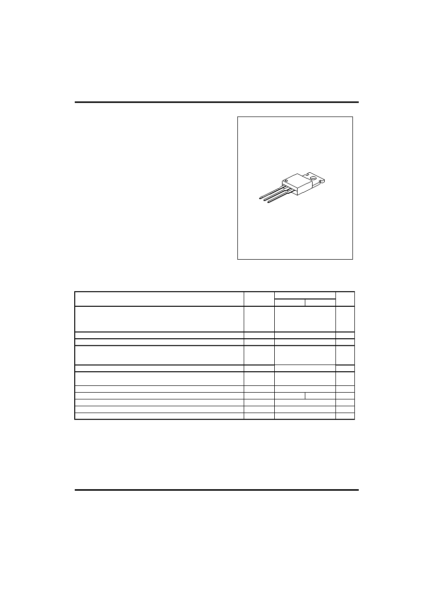
TO-220
1
1: CATHODE 2: ANODE 3: GATE
ABSOLUTE MAXIMUM RATINGS
RATING
PARAMETER SYMBOL
US112S US112N
UNIT
Repetitive peak off-state voltages
US112S/N-4
US112S/N-6
US112S/N-8
V
DRM
V
RRM
400
600
800
V
RMS on-state current (180� conduction angle) (Tc = 105�C)
I
T(RMS)
12 A
Average on-state current (180� conduction angle) (Tc = 105�C)
I
T(AV)
8 A
Non repetitive surge peak on-state current (Tj = 25�C)
tp=8.3ms
tp=10ms
I
TSM
146
140
A
I�t Value for fusing (tp = 10 ms, Tj = 25�C)
I�t
98
A�S
Critical rate of rise of on-state current
(IG = 2 x IGT , tr 100 n s, F = 60 Hz , Tj = 125�C,)
dI/dt 50
A/�s
Peak gate current (tp=20�s, Tj = 125�C)
I
GM
4
A
Maximum peak reverse gate voltage
V
RGM
5 V
Average gate power dissipation (Tj = 125�C)
P
G(AV)
1 W
Storage junction temperature range
Tstg
-40 ~ +150
�C
Operating junction temperature range
Tj
-40 ~ +125
�C
UTC US112S/N SCR
UTC
UNISONIC TECHNOLOGIES CO., LTD.
2
QW-R301-013,B
UTC US112S(SENSITIVE) ELECTRICAL CHARACTERISTICS
(Tj=25unless otherwise specified)
PARAMETER
SYMBOL
TEST CONDITIONS
MIN
MAX.
UNIT
Gate trigger Current
I
GT
V
D
= 12 V, R
L
=140
200
�A
Gate trigger Voltage
V
GT
V
D
= 12 V, R
L
=140
0.8 V
Gate non-trigger voltage
V
GD
V
D
= V
DRM,
R
L
= 3.3 k
, R
GK
= 1k
Tj = 125�C
0.1 V
Reverse gate voltage
V
RG
I
RG
= 10 �A
8
V
Holding Current
I
H
I
T
= 50 mA, R
GK
= 1 k
5
mA
Latching Current
I
L
I
G
= 1 mA ,R
GK
= 1 k
6
mA
Circuit Rate Of Change Of
off-state Voltage
dV/dt
V
D
= 67 % V
DRM
,
R
GK
= 220
Tj = 125�C
5
V/�s
On-state voltage
V
TM
I
TM
= 24A, t
p
= 380 �s,
Tj = 25�C
1.6 V
Threshold Voltage
V
t0
Tj = 125�C
0.85 V
Dynamic Resistance
R
d
Tj = 125�C
30 m
Off-state Leakage Current
I
DRM
I
RRM
V
DRM
= V
RRM,
R
GK
= 220
Tj = 25�C
Tj = 125�C
5
2
�A
mA
UTC US112N(STANDARD) ELECTRICAL CHARACTERISTICS
(Tj=25unless otherwise specified)
PARAMETER
SYMBOL
TEST CONDITIONS
MIN
MAX.
UNIT
Gate trigger Current
I
GT
V
D
= 12 V, R
L
=33
2 15
mA
Gate trigger Voltage
V
GT
V
D
= 12 V, R
L
=33
1.3 V
Gate non-trigger voltage
V
GD
V
D
= V
DRM,
R
L
= 3.3 k
,
Tj = 125�C
0.2 V
Holding Current
I
H
I
T
= 500 mA, Gate open
30
mA
Latching Current
I
L
I
G
= 1.2 I
GT
60
mA
Circuit Rate Of Change Of
off-state Voltage
dV/dt
V
D
= 67 % V
DRM
,
Gate open, Tj = 125�C
200 V/�s
On-state voltage
V
TM
I
TM
= 24A, t
p
= 380 �s,
Tj = 25�C
1.6 V
Threshold Voltage
V
t0
Tj = 125�C
0.85 V
Dynamic Resistance
R
d
Tj = 125�C
30 m
Off-state Leakage Current
I
DRM
I
RRM
V
DRM
= V
RRM,
Tj = 25�C
Tj = 125�C
5
2
�A
mA
THERMAL RESISTANCES
PARAMETER
SYMBOL
VALUE
UNIT
Junction to case (DC)
R
th(j-c)
1.3
KW
Junction to ambient
R
th(j-a)
60
K/W
UTC US112S/N SCR
UTC
UNISONIC TECHNOLOGIES CO., LTD.
3
QW-R301-013,B
12
9
10
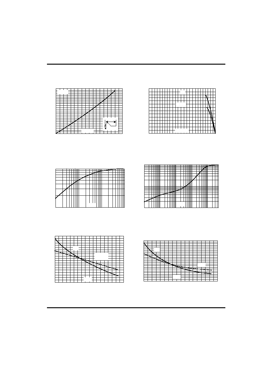
Figure.1:Maximum average power
dissipation vs average on-state current.
0
11
8
7
6
5
4
3
2
1
0
1
2
3
4
5
6
7
8
9
P(W)
360�
IT(av)(A)
=180�
14
12
Figure.2:Average and D.C. on-state current
vs case temperature
0
10
8
6
4
2
0
25
50
75
100
12
5
IT(av)(A)
=180�
Tcase()
DC
Fig.3-2:Relative variation of thermal impedance
junction to ambient vs pulseduration (recommended
pad layout,FR4 PC board)
2.0
1.6
Figure.4-1:Relative variation of gate trigger
current,holding current and latching vs
junction temperature (US112S)
-40
1.8
1.4
1.2
1.0
0.8
0.6
0.4
0.2
0.0
-20
0
20
40
60
80
100
120
140
IGT,IH,IL(TJ)/IGT,IH,IL (TJ=25)
Tj()
IGT
IH&IL
Rgk=1k
Fig.3-1:Relative variation of thermal impedance
junction to case vs pulse duration.
0.1
0.5
1.0
1E-2
1E-1
1E+0
1E-3
0.2
K=<Zth(j-c)/Rth(j-c)>
tp(s)
Figure.4-2: Relative variation of gate trigger
current,holding current and latching current vs
junction temperature (US112N).
2.4
1.8
2.0
-40
2.2
1.6
1.4
1.2
1.0
0.8
0.6
0.4
0.2
0.0
-20
0
20
40
60
80
100
120
140
IGT,IH,IL(TJ)/IGT,IH,IL (TJ=25)
Tj()
IGT
IH&IL
0.10
1.00
1E+2
1E-1
5E+2
1E-2
0.01
K=<Zth(j-a)/Rth(j-a)>
1E+0
1E+1
tp(s)

UTC US112S/N SCR
UTC
UNISONIC TECHNOLOGIES CO., LTD.
4
QW-R301-013,B
Fig.6: Relative variation of dV/dt immunity vs gate-
cathode resistance(typical values) (US112S)
0.1
10.0
1.0
0.2
0.0
dV/dt(Rgk)/dV/dt(Rgk=220)
1.0
0.8
0.6
0.4
1.2
Tj=125
VD=0.67* VDRM
Rgk()
Fig.7: Relative variation of dV/dt immunity vs gate-
cathode capacitance(typical values) (US112S)
0.0
4.0
2.0
25
0
dV/dt(Cgk)/dV/dt(Rgk=220)
125
100
75
50
150
VD=0.67* VDRM
Tj=125
Rgk=220
Cgk(nF)
0.5
1.0
1.5
2.5
3.0
3.5
Fig.8: Surge peak on-state current vs number of cycles
0.1
10.0
1.0
0.2
0.0
dV/dt(Rgk)/dV/dt(Rgk=220)
1.0
0.8
0.6
0.4
1.2
Tj=125
VD=0.67* VDRM
Rgk()
Fig.9:Non-repetitive surge peak on-state current for a
sinusoidal pulse with width tp<10ms, and corresponding
values of I t.
2
10
100
0.10
1.00
10.00
0.01
ITSM(A),I t(A s)
tp(ms)
2
2
1000
dI/dt
limitation
ITSM
Tjinitial=25
US112N
US112S
US112N
US112S
2000
Fig.10: On-state characteristics(maximum values).
Figure.5:Relative variation of holding current vs
gate-cathode resistance(typical values)
(US112S)
5.0
4.5
4.0
3.5
3.0
2.5
2.0
1.5
1.0
IH(Rgk)/IH(Rgk=1k)
1E-2
1E-1
1E+0
Rgk(k)
0.5
0.0
Ta=25
1E+1
I t
2
1
10
200
0.5
1.0
1.5
0.0
ITSM
100
4.5
4.0
3.5
3.0
2.5
2.0
5.0
VTM(V)
Tj=max:
Vto=0.85V
Rd=30m
Tj=25
Tj=Tjmax.