UTC 1812A/1812B/1813
CMOS IC
UTC
UNISONIC TECHNOLOGIES CO., LTD.
1
QW-R502-006,B
SINGLE SOUND GENERATOR
DESCRIPTION
The UTC 1812A/1812B/1813 is a CMOS LSI chip designed
for use in sound effect products .It is equipped with tone
circuit, noise circuit and other control logic to generate
different sounds including rifle gun, machine gun, booming
sound, door bell, alarm etc. The customer supplied sound
source can be analyzed and programmed into an internal
ROM by changing a mask layer during device fabrication. The
UTC 1812A/1812B/1813 is suitable for various toy
applications.
FEATURES
*Single power supply :2.4~3.3V
*Low standby current at 3V,1A typ
*Auto power-off function
*Speaker or direct piezo application
*Built-in envelope control circuit
*1Hz-8Hz programmable LED flash output
*Minimum external components
*Low operating current
*Strong driving capability
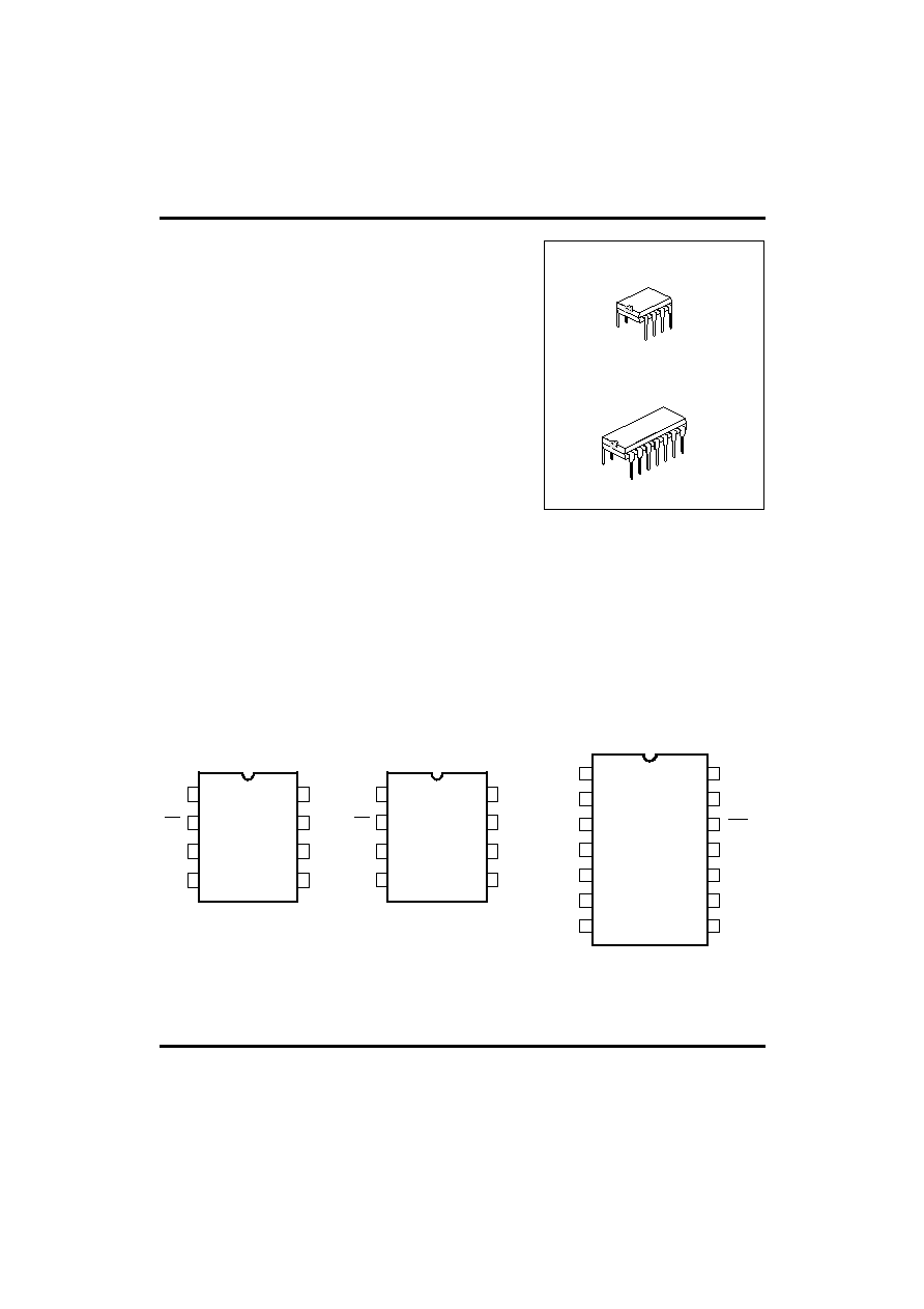
DIP-14
DIP-8
PIN CONFIGURATIONS
DIP-8
OSC1
1
2
3
4
7
6
5
KEY
OUT
VSS
VDD
8
OUT
LED
OSC2
1812A
DIP-8
OSC1
1
2
3
4
7
6
5
KEY
OUT
VSS
VDD
8
OUT
ENV
OSC2
1812B
DIP-14
1
2
3
4
7
6
5
TEST1
OSC1
V
DD
KEY
NC
TEST3
LED
OSC2
ENV
OUT
OUT
NC
VSS
TEST2
8
9
10
11
12
13
14
1813
UTC 1812A/1812B/1813
CMOS IC
UTC
UNISONIC TECHNOLOGIES CO., LTD.
2
QW-R502-006,B
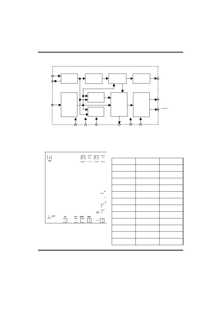
BLOCK DIAGRAM
Oscillator
Divider
Speed
Generator
LED
Divider
Key
Input
Logic
Tone
Generator
Noise
Generator
Selector &
Envelope
Circuit
Output
Divider
OSC1
OSC2
KEY
TEST1 TEST2 TEST3
ENV
VDD
VSS
OUT
OUT
LED
PAD COORDINATES
PAD No.
X
Y
1 90
1467
2 87 178
3 428 87
4 669 87
5 810 87
6 959 87
7 1241 87
8 1246 266
9 1251
1462
10 1109 1462
11 967 1462
(0,0)
12 823 1462
CHIP SIZE: 1.34 �1.56mm
SUBSTRATE: VDD
UTC 1812A/1812B/1813
CMOS IC
UTC
UNISONIC TECHNOLOGIES CO., LTD.
3
QW-R502-006,B
PAD DESCRIPTION
PAD No.
SYMBOL DESCRIPTION
1
VSS
Negative power supply, GND
2
OUT
Sound output pad, out of phase to pad 3
3
OUT
Sound output pad
4
ENV
Sound envelope control pad
5
TEST3
For IC test only
6
LED
LED flash output pad
7
VDD
Positive power supply
8
KEY
Key input pad, low active
9
OSC2
Oscillator output pad
10
OSC1
Oscillator input pad
11
TEST1
For IC test only
12
TEST2
For IC test only
ABSOLUTE MAXIMUN RATINGS
*
PARAMETER SYMBOL
VALUE UNIT
Supply Voltage
Vcc
-0.3~5
V
Input Voltage
V
IN
Vss-0.3 ~ V
DD
+0.3 V
Operating Temperature
Topr
0~70
�C
Storage Temperature
Tstg
-50~125
�C
*Note: Stresses above those listed under "Absolute Maximum Ratings" may cause permanent damage to the device.
These are stress ratings only. Functional operation of this device at these or any other conditions above those
indicated in the operational sections of this specification is not implied and exposure to absolute maximum rating
conditions for extended periods may affect device reliability.
ELECTRICAL CHARACTERISTICS
PARAMETER SYMBOL TEST
CONDITIONS MIN
TYP
MAX
UNIT
Operating Voltage
V
DD
V
DD
=3V
2.4
3
3.3
V
Standby Current
I
STB
V
DD
=3V
1
5
A
Operating Current
I
DD
V
DD
=3V, NO LOAD
300
600
A
Output Source Current
I
OH
V
DD
=3V, V
OH
=2.5V -1
-2
mA
Output Sink Current
I
OL
V
DD
=3V, V
OL
=0.5V 1
2
mA
ENV Source Current
I
ENV
V
DD
=3V, V
OH
=2.5V -1
-2
mA
LED Source Current
I
LED
V
DD
=3V, V
OH
=2.5V -1
-2
mA
Oscillator Frequency
F
OSC
R=330k
64
kHz
UTC 1812A/1812B/1813
CMOS IC
UTC
UNISONIC TECHNOLOGIES CO., LTD.
4
QW-R502-006,B
PARAMETER SYMBOL TEST
CONDITIONS MIN
TYP
MAX
UNIT
"H" Input Voltage
V
IH
V
DD
=3V
2.4
V
"L" Input Voltage
V
IL
V
DD
=3V
0.6
V
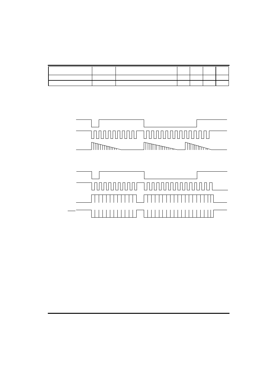
TIMING DIAGRAM
With an envelope
KEY
OSCILLATOR
OUT
No envelope
OSCILLATOR
OUT
KEY
OUT
UTC 1812A/1812B/1813
CMOS IC
UTC
UNISONIC TECHNOLOGIES CO., LTD.
5
QW-R502-006,B
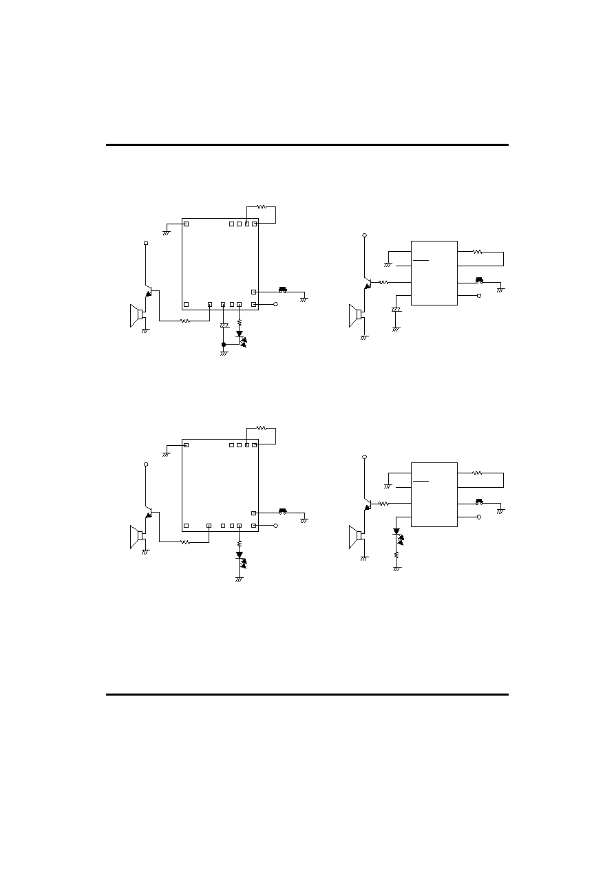
APPLICATION CIRCUITS
Speaker output with an envelope
1812B
1
2
3
4 5 6
7
8
Rosc
VDD
KEY
8050
VDD
100
100
33
+
121110 9
*The IC substrate should be connected to VDD in the PCB layout artwork.
8050
VDD
VDD
100
33
+
Rosc
1
2
3
4
5
6
7
8
VDD
KEY
OSC2
OSC1
VSS
OUT
OUT
ENV
1812B
Speaker output without an envelope
1812A
1
2
3
4 5 6
7
8
Rosc
VDD
KEY
8050
VDD
100
100
121110 9
*The IC substrate should be connected to VDD in the PCB layout artwork.
8050
VDD
VDD
100
Rosc
1
2
3
4
5
6
7
8
VDD
KEY
OSC2
OSC1
VSS
OUT
OUT
LED
100
1812A