 | –≠–ª–µ–∫—Ç—Ä–æ–Ω–Ω—ã–π –∫–æ–º–ø–æ–Ω–µ–Ω—Ç: UTCLP2950 | –°–∫–∞—á–∞—Ç—å:  PDF PDF  ZIP ZIP |

UTC LP2950/2951 LINEAR INTEGRATED CIRCUIT
UTC
UNISONIC TECHNOLOGIES CO., LTD.
1
QW-R102-001,E
100 mA LOW-DROPOUT VOLTAGE
REGULATOR
DESCRIPTION
The UTC LP2950/2951 is a monolithic integrated voltage
regulator with low dropout voltage, and low quiescent current.
It includes many features that suitable for different
applications. Available in 3-pin TO-92, DIP-8 and SOP-8
packages.
FEATURES
*High accuracy 2.5, 3.0, 3.3, 3.6 or 5V fixed output for
TO-92, SOP-8 package.
*Extremely low quiescent current and dropout voltage.
*Extremely tight load and line regulation.
*Current and thermal limiting.
*Very low temperature coefficient.
*Logic controlled shutdown and error flag available for DIP
and SOP package.
*Output voltage programmable for DIP and SOP package.
APPLICATIONS
*Battery powered equipment.
*High efficient linear regulator down to 1.24V.
*Cellular phones.
TO-92
SOP-8
DIP-8
1
ORDERING INFORMATION
PART NUMBER
TEMPERATURE RANGE PACKAGE
ACCURACY
UTC LP2950-5.0
-40 ~ +125
∞C
3-Pin TO-92 plastic
2.0%
UTC LP2950-3.0
-40 ~ +125
∞C
3-Pin TO-92 plastic
1.0%
UTC LP2950-3.3
-40 ~ +125
∞C
3-Pin TO-92 plastic
1.0%
UTC LP2950-3.6
-40 ~ +125
∞C
3-Pin TO-92 plastic
2.0%
UTC LP2950-2.5
-40 ~ +125
∞C
3-Pin TO-92 plastic
1.0%
UTC LP2950-5.0
-40 ~ +125
∞C
8-Pin SOP-8 plastic
2.0%
UTC LP2950-3.0
-40 ~ +125
∞C
8-Pin SOP-8 plastic
1.0%
UTC LP2950-3.3
-40 ~ +125
∞C
8-Pin SOP-8 plastic
1.0%
UTC LP2951
-40 ~ +125
∞C
8-Pin SOP-8 plastic
2.0%
UTC LP2951
-40 ~ +125
∞C
8-Pin DIP-8 plastic
2.0%
UTC LP2950/2951 LINEAR INTEGRATED CIRCUIT
UTC
UNISONIC TECHNOLOGIES CO., LTD.
2
QW-R102-001,E
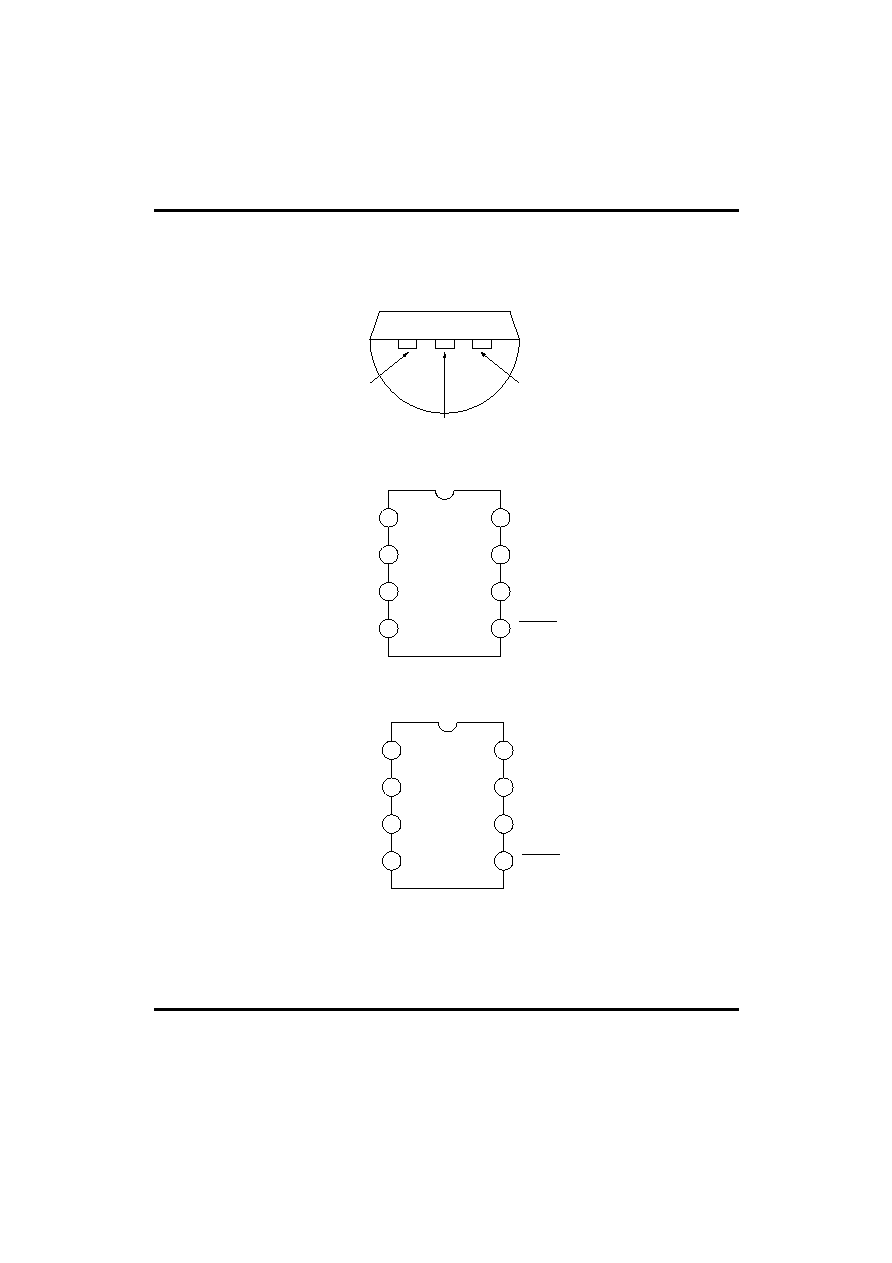
PIN CONFIGURATIONS
2
1 3
OUTPUT
GND
INPUT
UTC LP2950
TO-92 Plastic Package
Bottom View
1
2
3
4
8
7
6
5
INPUT
FEEDBACK
5V TAP
SHUTDOWN
SENSE
OUTPUT
UTC
LP2951
GND
ERROR
SOP-8 OR DIP-8 PACKAGE
FOR UTC LP2951
1
2
3
4
8
7
6
5
INPUT
NC
NC
SHUTDOWN
NC
OUTPUT
UTC
LP2950
GND
ERROR
SOP-8 OR DIP-8 PACKAGE
FOR UTC LP2950
Fig.1

UTC LP2950/2951 LINEAR INTEGRATED CIRCUIT
UTC
UNISONIC TECHNOLOGIES CO., LTD.
3
QW-R102-001,E
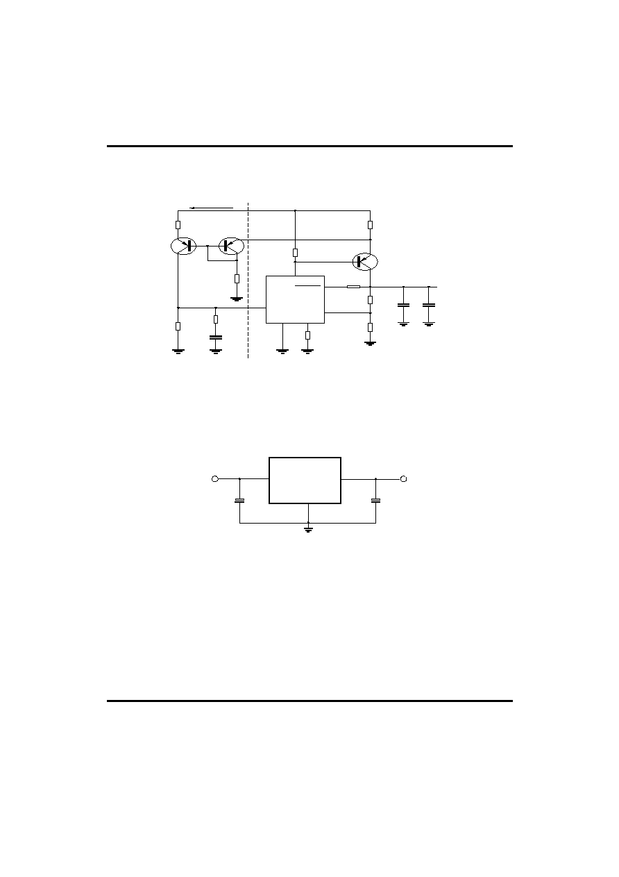
BLOCK DIAGRAM
5
4
6
2
1
8
7
3
60mV
330K
TO CMOS
OR TTL
5V 150mA
MAX.
FEEDBACK
INPUT
OUTPUT
SENSE
5V TAP
GND
ERROR
DETECTION
COMPARATOR
ERROR
AMPLIFIER
FROM CMOS
OR TTL
1.23
REF
SHUT
DOWN
UNRAGULATED
DC
ERROR
182k
60k
1.5
µF
FOR UTC LP2951
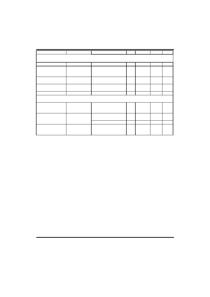
ABSOLUTE MAXIMUM RATINGS
PARAMETER
SYMBOL VALUE
UNIT
Supply Voltage
Vcc
-0.3~+18
V
Feedback Voltage
Vfeedback
-1.5~+18
V
Shutdown Voltage
Vshutdown
-0.3~+18
V
Comparator Output Voltage
Vco
-0.3~+18
V
Storage Temperature
Tstr
-65~+150
∞C
Operating Junction Temperature
Tj
-40~+125
∞C

UTC LP2950/2951 LINEAR INTEGRATED CIRCUIT
UTC
UNISONIC TECHNOLOGIES CO., LTD.
4
QW-R102-001,E
ELECTRICAL CHARACTERISTICS
(Tested at Tj=25
∞C,V
IN
=6V,I
L
=100
µA and C
L
=1
µF, unless otherwise specified)
PARAMETER
PART NUMBER
TEST CONDITION
MIN.
TYP. MAX.
UNIT
Output Voltage
UTC LP2950-2.5
UTC LP2950-3.0
UTC LP2950-3.3
UTC LP2950-3.6
UTC LP2950-5.0
UTC LP2951
T
J
=25
∞C
(note 1)
2.47
2.97
3.27
3.53
4.90
2.5
3.0
3.3
3.6
5.0
2.53
3.03
3.33
3.67
5.10
V
UTC
LP2950-2.5
UTC LP2950-3.0
UTC LP2950-3.3
UTC LP2950-3.6
UTC LP2950-5.0
UTC LP2951
-25
∞C<=T
J<=
<=+85
∞C
(note 1)
2.47
2.97
3.27
3.53
4.90
2.5
3.0
3.3
3.6
5.0
2.53
3.03
3.33
3.67
5.10
V
Output Voltage
UTC LP2950-2.5
UTC LP2950-3.0
UTC LP2950-3.3
UTC LP2950-3.6
UTC LP2950-5.0
UTC LP2951
100
µA<=I
L
<=100 mA
Tj<=Tj(max)
(note 1)
2.47
2.97
3.27
3.53
4.90
2.5
3.0
3.3
3.6
5.0
2.53
3.03
3.33
3.67
5.10
V
Output Voltage
Temperature Coefficient
20
100
ppm/
∞C
Line Regulation
6V<=V
IN
<=18V 0.03
0.1
0.2
%
Load Regulation
100
µA<=I
L
<=100 mA
0.04
0.1 0.2
%
Dropout Voltage
I
L
=100
µA
I
L
=100mA (note 2)
50
380
80
450
150
600
mV
Ground Current
I
L
=100
µA
I
L
=100mA
75
8
120
12
140
14
µA
mA
Dropout Ground Current
V
IN
=4.5V,I
L
=100
µA
110
170 200
µA
Current Limit
Vout=0
160
200
220
mA
Output Noise 10Hz to
100KHz
C
L
=1
µF
C
L
=200
µF
C
L
=3.3
µF
(Bypass=0.01
µF
pins 7 to (
utc
2951))
430
160
100
µV
For LP2951 8-Pin version only
Reference Voltage
1.22
1.235
1.25
V
Reference Voltage
(Note 4)
1.19
1.27
V
Feedback pin Bias
Current
20
40
nA
Reference Voltage
Temperature Coefficient
50
ppm/
∞C
Feedback Bias Current
temperature Coefficient
0.1
nA/
∞C
UTC LP2950/2951 LINEAR INTEGRATED CIRCUIT
UTC
UNISONIC TECHNOLOGIES CO., LTD.
5
QW-R102-001,E
PARAMETER
PART NUMBER
TEST CONDITION
MIN.
TYP. MAX.
UNIT
Error Comparator
Output Leakage Current
V
OH
=18V
1
µA
Output Low Voltage
V
IN
=4.5V
I
OL
=400
µA
250
mV
Upper Threshold
Voltage
(Note
3) 3.2
%V
O
Lower Threshold
Voltage
(Note
3)
7.6
%V
O
Hysteresis
(Note
3)
15
mV
Shutdown Input
Input Logic Voltage
Low(Regulator ON)
High(Regulator OFF)
2.0
1.3
0.70
V
Shutdown Pin Input
Current
V
shutdown
=2.4V
30 50
µA
V
shutdown
=18V
450
600
µA
Regulator Output
Current Shutdown
Vshutdown>=2V,V
IN
<=18V,
V
out
=0,
Feedback pin tied to 5V Tap.
3 10
µA
Note 1: Additional conditions for 8-pin versions are feedback tied to 5V Tap an Output tied to Output Sense
(V
out
=5V) and Vshutdown<=0.8V.
Note 2:Dropout Voltage is defined as the input to output differential at which the output voltage drops 100mV
below its nominal value measured at 1V differential.
Note 3:Comparator thresholds are expressed in terms of percentage value of voltage output.
Note 4:Vref
Vout(Vin-1V), 2.3VVin30V, 100µAI
L
100mA, T
J
T
JMAX
UTC LP2950/2951 LINEAR INTEGRATED CIRCUIT
UTC
UNISONIC TECHNOLOGIES CO., LTD.
6
QW-R102-001,E
APPLICATION CIRCUIT
(10 Ampere Low Dropout Regulator)
+V
IN
FB
Vout
GND
SD
ERROR
UTC LP2951
8
5
7
1
4
3
CURRENT
LIMIT
SECTION
+V
IN
=V
ou
t+0.5V
0.05
470
680
4.7M
20k
220
0.033
µF
47
R1
R2
4.7
µF
100
µF
1%
10k
2N3906
+
V
OUT
100m A
Vout=1.23V*(1+R1/R2)
For 5V output
use internal resistors.Wire pin 6 to 7
and wire pin 2 to +V
out
UTC
D65H0
Fig.2
UTC LP2950-2.5
UTC LP2950-3.0
UTC LP2950-3.3
UTC LP2950-3.6
UTC LP2950-5.0
Vin
Vout
Fig.3

UTC LP2950/2951 LINEAR INTEGRATED CIRCUIT
UTC
UNISONIC TECHNOLOGIES CO., LTD.
7
QW-R102-001,E
TYPICAL PERFORMANCE CHARACTERISTICS
1
2
3
4
5
6
0
0
1
2
3
4
5
6
Fig.4 Dropout Characteristics
INPUT VOLTAGE(V)
O
U
T
P
U
T
VO
L
T
AG
E(
V)
R
L
=50k
R
L
=50
0 1
2
3 4
5 6
7 8
9 10 11 12
0
10
20
30
40
50
60
70
80
90
100
120
110
130
140
150
Fig.5 Input Current
I
N
PUT CURRENT(
m
A)
INPUT VOLTAGE(V)
R
L
=50
50
60
70
80
90
100
110
120
-75 -50 -25
0
25
50 75
100 125 150
Fig. 7 Ground Pin Current
QUI
ESCENT CURRENT(
m
A)
TEMPERATURE(∞C)?
V
IN
=6V
I
L
=100
µA
-75 -50 -25
0
25
50 75
100 125 150
4
5
6
7
8
TEMPERATURE(∞C)?
Fig. 8 Ground Pin Current
QUI
ESCENT CURRENT(
m
A)
V
IN
=6V
I
L
=100mA
-75 -50 -25
0
25
50 75
100 125 150
100
110
120
130
140
150
160
170
TEMPERATURE(∞C)?
SHORT CI
RCUI
T CURRENT(
m
A)
Fig. 10 Short Circuit Current
-75 -50 -25
0
25
50 75
100 125 150
0
50
100
300
400
500
600
TEMPERATURE(∞C)?
DROPOUT VOL
T
AGE(
mV)
Fig. 6 Dropout Voltage
I
L
=100mA
I
L
=100
µA
-75 -50 -25
0
25
50 75
100 125 150
TEMPERATURE(∞C)
0.6
0.8
1.0
1.2
1.4
1.6
1.8
Fig. 9 Shutdown Threshold Voltage
S
hut
down T
h
r
e
s
hold V
o
lt
age(
V
)
0.1
1
10
100
0
100
200
300
400
500
Fig. 11 Dropout Voltage
OUTPUT CURRENT(mA)
D
r
opout
V
o
l
t
age(m
V
)