 | –≠–ª–µ–∫—Ç—Ä–æ–Ω–Ω—ã–π –∫–æ–º–ø–æ–Ω–µ–Ω—Ç: UTCRCR02 | –°–∫–∞—á–∞—Ç—å:  PDF PDF  ZIP ZIP |
UTC RCR02
CMOS IC
UTC
UNISONIC TECHNOLOGIES CO., LTD.
1
QW-R502-001,B
Decoder For Remote Controller
With Five Functions
DESCRIPTION
The chip can be used with the encoder RCT02 to provide a
complete control functions to the remote-controlled toy. The
RCR02 has five output pins corresponding with the five
function actions i.e, forward, backward, rightward, leftward
and turbo. The received signals are amplified by the
three-stage amplifier, and then the appropriate amplified
signals are sampled, fault-tolerantly checked and decoded to
control the actions of the remote-controlled toy.
There is an internal oscillator in the RCR02.By adding an
external resistor conveniently, the oscillator will be
constructed. The oscillator frequency can be adjusted by the
external resistor.The relative error between the frequencies of
the two on chip oscillators in the RCT02 and RCR02 must be
less than ±25%.
FEATURES
*Five output pins for control functions
*Operating power-supply voltage range: 2.5 to 5.0V
*On-chip reversing amplifiers
*On-chip oscillator with an external resistor
*Low operating current
*Few external components needed
DIP-16
SOP-16
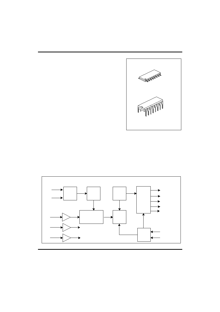
LOGIC BLOCK DIAGRAM
TURBO
OSCI
Oscillator
Timing
Generator
Latch
Decoding
Circuit
Signal Sample
and Fault-
Tolerant Check
Output
Circuit
Amp
Amp
Amp
OSCO
SI
VI1
VI2
VO1
VO2
RIGHT
FORWARD
BACKWARD
LEFT
Control
Logic
LDB
RDB
UTC RCR02
CMOS IC
UTC
UNISONIC TECHNOLOGIES CO., LTD.
2
QW-R502-001,B
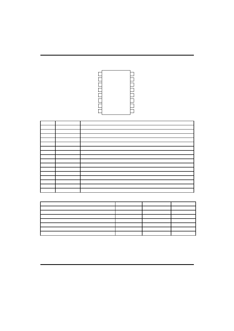
PRODUCT PIN CONFIGURATION AND DESCRIPTION
RIGHT
OSCI
OSCO
SI
VI1
VI2
VO1
VO2
TURBO
FORWARD
LDB
BACKWARD
LEFT
1
2
3
4
5
6
7
8
16
15
14
13
12
11
10
9
RDB
GND
VDD
Pin No.
Pin Name
Description
1
VO2
Output pin for the amplifier 2
2
GND
Negative power supply
3
SI
Input pin of the encoding signal
4
OSCI
Oscillator input pin
5
OSCO
Oscillator output pin
6
RIGHT
Rightward output pin
7
LEFT
Leftward output pin
8
RDB
Rightward function disable, if this pin is connected to GND
9
LDB
Leftward function disable, if this pin is connected to GND
10
BACKWARD
Backward output pin
11
FORWARD
Forward output pin
12
TURBO
Turbo output pin
13
VDD
Positive power supply
14
VI1
Input pin for the amplifier 1
15
VO1
Output pin for the amplifier 1
16
VI2
Input pin for the amplifier 2
ABSOLUTE MAXIMUM RATINGS
PARAMETER SYMBOL
VALUE
UNIT
DC Input Voltage
V
IN
-0.5 ~ +5.5
V
Supply Voltage to Ground Potential(Inputs &V
DD
Only)
-0.5 ~ +5.5
V
Supply Voltage to Ground Potential(Outputs &D/O
Only)
-0.5 ~ +5.5
V
DC Output Current
Io
20
mA
Power Dissipation
P
D
500
mW
Ambient Temperature With Power Applied
T
A
-10 ~ +40
∞C
Storage Temperature
T
STG
-25 ~ +85
∞C
UTC RCR02
CMOS IC
UTC
UNISONIC TECHNOLOGIES CO., LTD.
3
QW-R502-001,B
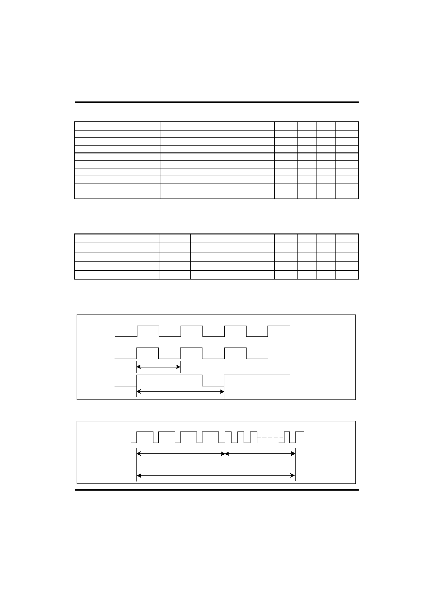
DC ELECTRICAL CHARACTERISTICS
(Over the operating rating,T
A
= -10
∞C~ +40∞C,V
DD
=4.0V±10%)
PARAMETER
SYMBOL
TEST CONDITIONS
MIN
TYP MAX UNITS
Operating Voltage
V
DD
2.5 4.0 5.0 V
Supply Current
I
DD
*
3.0 mA
Input Current
I
IN
For RDB and LDB pins
60
µA
Input Low Voltage
V
IL
For RDB and LDB pins
0.5
V
Input High Voltage
V
IH
For RDB and LDB pins
3.5
V
Output High Voltage
V
OH
I
OUT
=400
µA 3.5
V
Output High Current
I
OH
V
OUT=
1.4V -1.5
mA
Output Low Voltage
V
OL
I
OUT
=1.0mA
0.5 V
Output Low Current
I
OL
V
OUT=
0.5V 1.0
mA
Note*:Output unlosded; 2.2Mfeedback resistors for the two reversing amplifiers; 200K external resistor for the
on-chip oscillator.
AC ELECTRICAL CHARACTERISTICS
(Over the operating rating, T
A
= -10
∞C~ +40∞C,V
DD
=4.0V±10%)
PARAMETER
SYMBOL
TEST CONDITIONS
MIN
TYP MAX UNITS
Oscillator Frequency*
Fosc
T
A
=25
∞C,R=200K
102
128
154
KHz
SI Pin Vpp Receive Sensitivity
V
SI
Guaranteed Effective Decoding
300
mV
Cycle Time of Function Code
T
FUN
F
OSC
=128KHz 0.75
1
1.25
ms
Cycle Time of Start Code
T
STA
F
OSC
=128KHz 1.5
2
2.5
ms
Note*:The relative error between the frequencies of the two on-chip oscillators in the RCT02 and RCR02 must be
less than±25%
BIT FORMAT FOR THE RECEIVED SIGNAL
(W1 is used for function codes,W2 for start codes)
W1
W1:1KHz 50% Duty Cycle Typical
W2
W2: 500Hz 75% Duty Cycle Typical
WORD FORMAT FOR RECEIVED SIGNAL
Start Code: 4 ' W2
Function Code: n ' W1
1 Word
UTC RCR02
CMOS IC
UTC
UNISONIC TECHNOLOGIES CO., LTD.
4
QW-R502-001,B
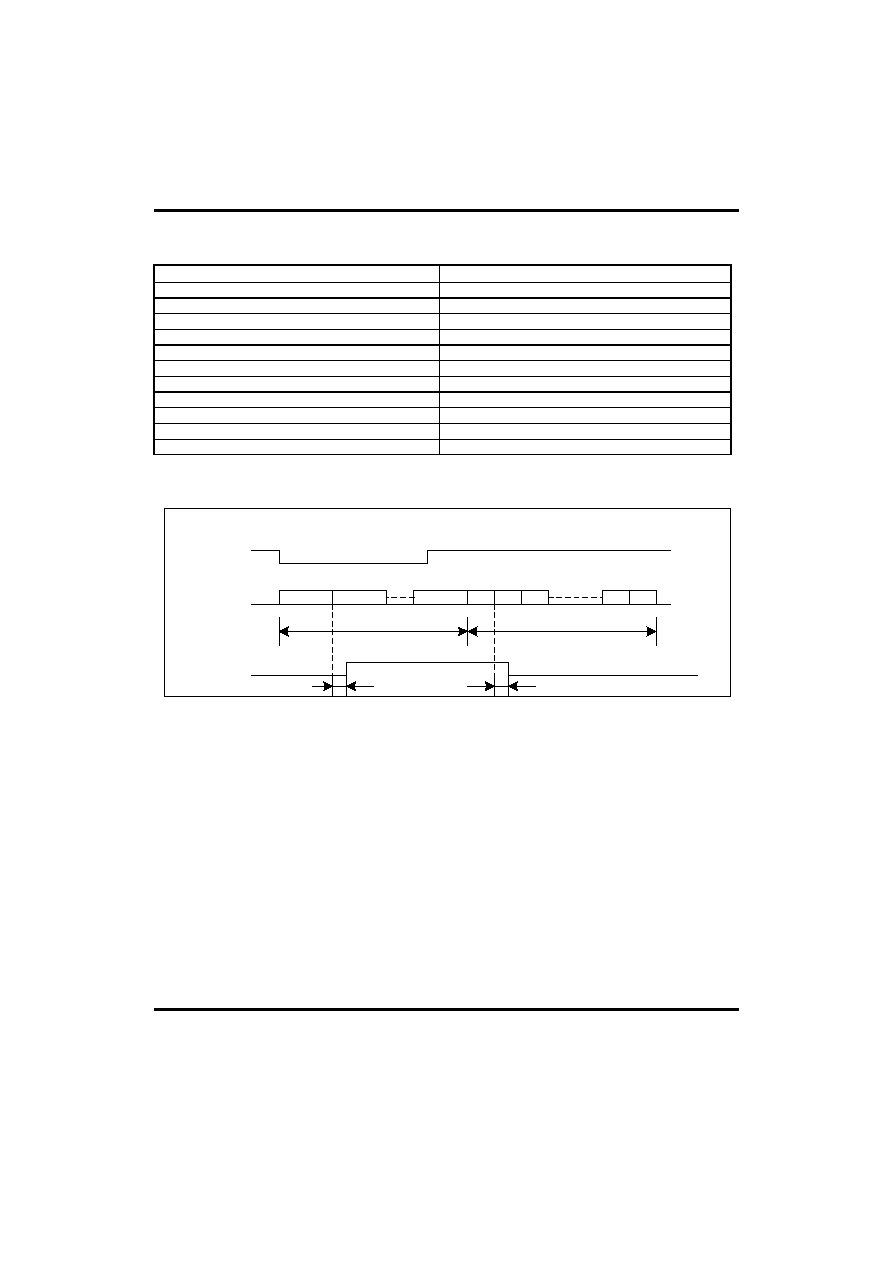
ENCODING INPUT FORMAT AND DECODING RESULT
W2 W2 W2 W2 (n)' W1 W2 W2 W2 W2 (n)' W1 W2 W2 W2 W2 (n)' W1 W2 W2 W2 W2 (n)'W1- - - - - - - -
Number of Function Codes(n)W1
Decoding Result
4 End
Code
10 Forward
16 Forward
22 Turbo
28
Forward & Left
34
Forward & Right
40 Backward
46
Backward & Right
52
Backward & Left
58 Left
64 Right
DECODING TIMING
Press any buttons
on RCT02
Encoding output
from RCT02
1st word 2nd word
Function Codes
End Codes
last word
1
2
3
14
15
Decoding output
from RCR02
9ms
9ms
UTC RCR02
CMOS IC
UTC
UNISONIC TECHNOLOGIES CO., LTD.
5
QW-R502-001,B
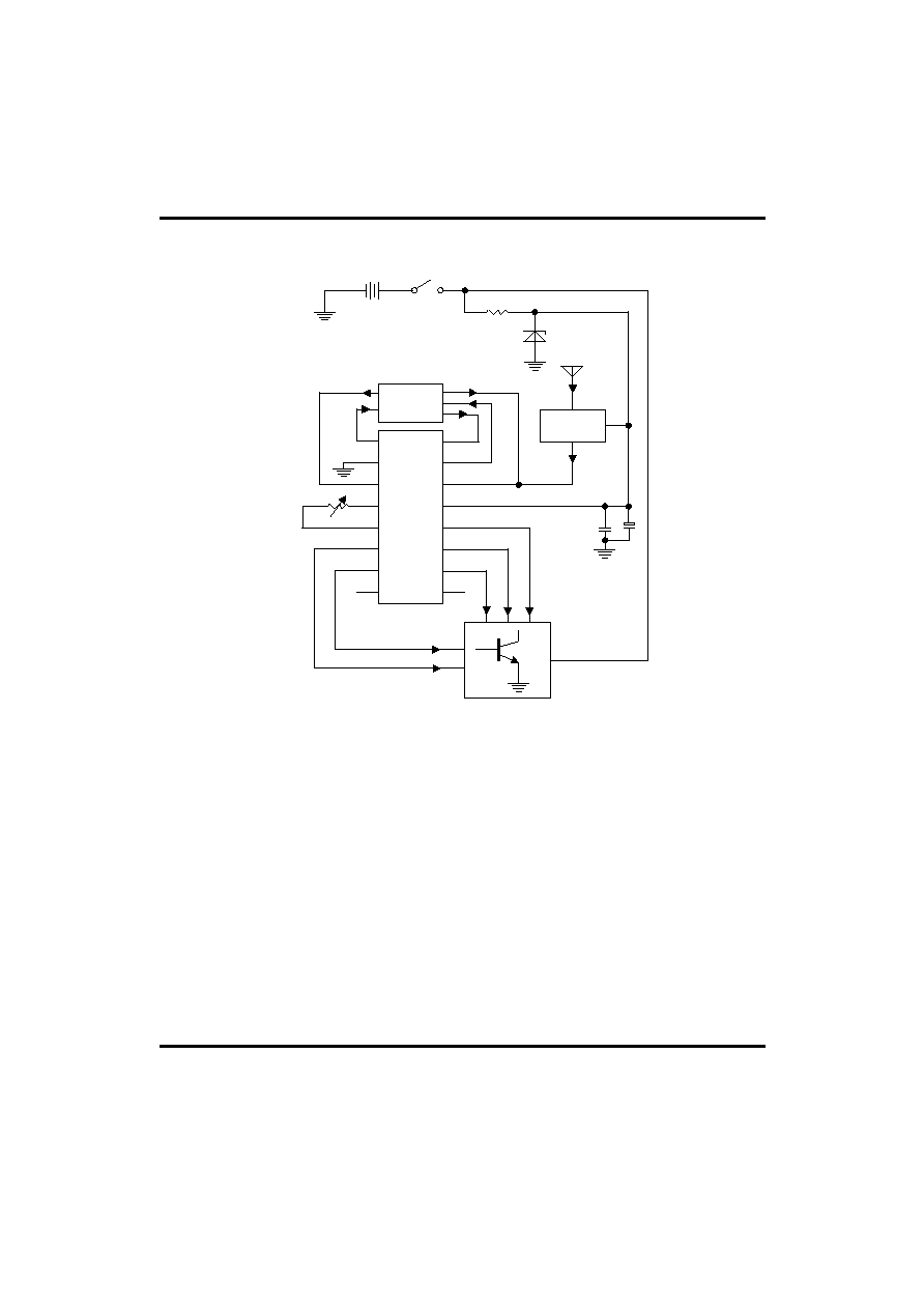
BLOCK DIAGRAM OF APPLICATION CIRCUIT
MOTOR DRIVING
CIRCUITS
1
2
3
4
5
6
7
8
16
15
14
13
12
11
10
9
VO2
VO1
VI2
VI1
RDB
GND
TURBO
SI
VDD
OSCI
FOR
RIGHT
OSCO
LEFT
BACK
LDB
+
BATTERY
FEEDBACK
AND
FILTER
RF
RECEIVER
RCR02