
UTC TA8227P LINEAR INTEGRATED CIRCUIT
UTC
UNISONIC TECHNOLOGIES CO., LTD.
1
QW-R107-011,B
LOW FREQUENCY POWER
AMPLIFIER
DESCRIPTION
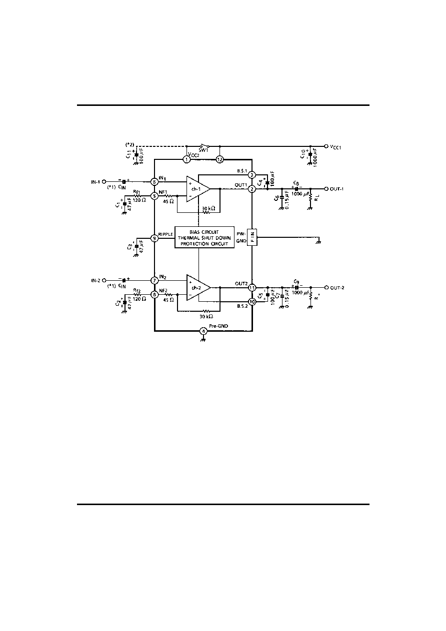
The UTC TA8227P is an audio power IC with built-in two
channels developed for portable radio cassette tape recorder
with power ON / OFF switch.
Because of the parts reduction and DIP, space merit is
remarkable.
Thermal shut down protection circuit is built in.
FEATURES
*Wide operating supply voltage: Vcc=5~12V
*Low popping noise at power ON
*Best for supply voltage 9V
*Output power
Po=2.5W/CH at Vcc=9V, R
L
=4
, f=1kHz, THD=10%
Po=3.0W/CH at Vcc=9V, R
L
=3
, f=1kHz, THD=10%
*Soft Clip
*Built-in Thermal shut-down protection circuit
*Stand-by Switch
DIP-12H
BLOCK DIAGRAM
UTC TA8227P LINEAR INTEGRATED CIRCUIT
UTC
UNISONIC TECHNOLOGIES CO., LTD.
2
QW-R107-011,B
APPLICATION INFORMATION AND APPLICATION METHOD
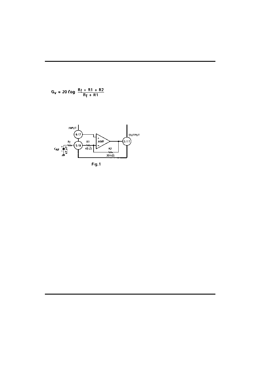
1. Adjustment of voltage gain
The voltage gain Gv is obtained as follows by R1, R2 and Rf in Fig.1
When Rf=0
Gv=56.5 dB (Typ.)
When Rf=120
Gv=45 dB (Typ.)
By increasing Rf, reduction of Gv is possible. However, since the feedback increase is liable to produce
oscillation, it is recommended to use this at 40dB or over.
2. Thermal shut-down circuit
The thermal shut-down circuit is built in for the purpose of preventing the destruction of IC due to the abnormal
temperature rise when the heat radiation is insufficient.
The operation temperature is set at radiation Fin temperature 175
�C (Typ.)
At this temperature or over the bias is interrupted to prevent the destruction of IC.
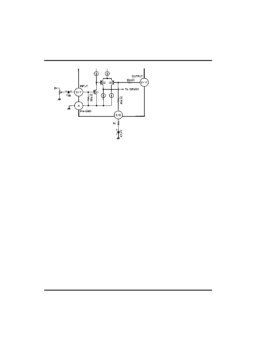
3. Input stage
The input circuit of this IC is as shown in fig.2. PNP Tr : Q1 is provided in the input circuit so as to make its usage
possible without the input coupling capacitor.
However, at pin 6 and pin 7, max 60mV offset voltage is produced.
Application after checking volume slide noise is recommended.
For cutting the volume slide noise, insert the input capacitor: C
IN
in series to interrupt the DC component.
UTC TA8227P LINEAR INTEGRATED CIRCUIT
UTC
UNISONIC TECHNOLOGIES CO., LTD.
3
QW-R107-011,B
4.
Oscillation
preventive measures
For oscillation preventive capacitor C6 and C7 between the output terminal and GND, it is recommended to use
polyester film capacitor having good characteristics for temperature and for high frequency.
Since the characteristics of the capacitor is liable to be influenced by the temperature, use this capacitor after the
temperature test to check the oscillation allowance.
In addition, as the position of the electrolytic capacitor has a remarkable influence on the oscillation, connect C10
to Vcc at the nearest possible position from power GND.
At using this application wth the voltage gain reduced, oscillation is liable to be produced. Apply the capacitor
after checking enough for its capacity, type and mounting position.
5. Power ON / OFF switch
There is power ON / OFF switch at Pin1. However, output power is changed by Pin1 supply voltage when Pin1
supply voltage is not same Pin12 supply voltage, after referring to attached date, select Pin1 supply voltage.
6. Input voltage
When the excessive signal is input, turning-up is produced in the clip waveform. The turning-up point is
Vin=300mVrms (Typ.) : Vcc=9V, RL=4
, f=1kHz : Enough care must be taken for this phenomenon.
UTC TA8227P LINEAR INTEGRATED CIRCUIT
UTC
UNISONIC TECHNOLOGIES CO., LTD.
4
QW-R107-011,B
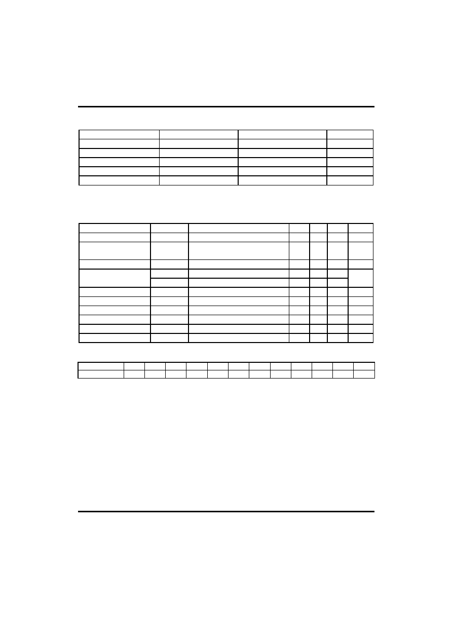
ABSOLUTE MAXIMUN RATINGS
(Ta=25
�C)
PARAMETER SYMBOL
VALUE UNIT
Supply Voltage
Vcc
20
V
Output Current (peak / CH)
Io (peak)
2.5
A
Power Dissipation
Pd
4.0
W
Operating Temperature
Topr
-25~75
�C
Storage Temperature
Tstg
-55~150
�C
ELECTRICAL CHARACTERISTICS
(Ta=25
�C, Vcc=9V, R
L
=4
, R
g
=600
, f=1kHz, unless otherwise specified)
PARAMETER SYMBOL TEST
CONDITIONS MIN
TYP
MAX
UNIT
Quiescent Current
I
CCQ
Vin=0
21
45
mA
Output Power
Pout(1)
Pout(2)
THD=10%
THD=10%, RL=3
2.0
2.5
3.0
W
Total Harmonic Distortion
THD
Pout=0.4W/CH
0.2
1.0
%
Voltage Gain
Gv1
Rf=120
,Vout=0.775Vrms (0 dBm)
43 45 47 dB
Gv2
Rf=0, Vout=0.775Vrms (0 dBm)
56.5
Input Impedance
Rin
30
k
Output Noise Voltage
Vno
Rg=10k
,BW=20Hz~20kHz
0.3
1.0
mVrms
Ripple Rejection Ratio
R.R.
Rg=600
, fripple=100Hz
-52 dB
Cross Talk
C.T
Rg=600
,Vout=0.775Vrms (0 dBm)
-50 dB
Input Offset Voltage
V6, V7
30
60
mV
Standby
Current
1stb
Sw1:OFF
1
�A
TYP. DC VOLTAGE OF EACH TERMINAL
(Vcc=9V, Ta=25
�C )
TERMINAL
NO.
1 2 3 4 5 6 7 8 9 10
11
12
DC VOLTAGE (V)
Vcc
4.5
8.7
GND
0.7
0.03
0.03
0.7
5.0
8.7
4.5
Vcc
UTC TA8227P LINEAR INTEGRATED CIRCUIT
UTC
UNISONIC TECHNOLOGIES CO., LTD.
5
QW-R107-011,B
TEST CIRCUIT
Note 1: This IC can be used without coupling capacitor (C
IN
). If volume slide noise noise occurred by input offset
voltage is undesirable, it needs to use the capacitor (C
IN
).
Note 2: The condenser between the pin4 and the GND (C11) is for reducing pop noise when the power ON / OFF
switch (SW1) is set to ON / OFF.

UTC TA8227P LINEAR INTEGRATED CIRCUIT
UTC
UNISONIC TECHNOLOGIES CO., LTD.
6
QW-R107-011,B

UTC TA8227P LINEAR INTEGRATED CIRCUIT
UTC
UNISONIC TECHNOLOGIES CO., LTD.
7
QW-R107-011,B

UTC TA8227P LINEAR INTEGRATED CIRCUIT
UTC
UNISONIC TECHNOLOGIES CO., LTD.
8
QW-R107-011,B
UTC TA8227P LINEAR INTEGRATED CIRCUIT
UTC
UNISONIC TECHNOLOGIES CO., LTD.
9
QW-R107-011,B
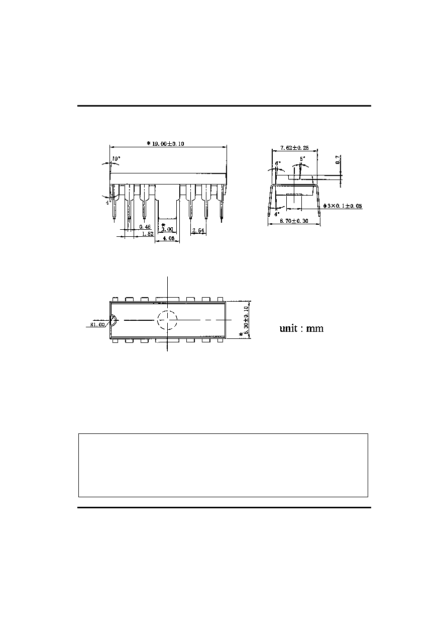
PACKAGE DIMENSION
Remark: The "
" means quality inspection range.
l The information contained herein is presented only as a guide for the applications of our products. No
responsibility is assumed by UNISONIC TECHNOLOGIES CO., LTD. for any infringements of intellectual
property or other rights of the third parties, which may result from its use. No license is granted by
implication or otherwise under any intellectual property or other rights of UNISONIC TECHNOLOGIES CO.,
LTD. or others.