UTC TDA7088
LINEAR INTEGRATED CIRCUIT
UTC
UNISONIC TECHNOLOGIES CO., LTD.
1
QW-R110-016,A
FM RECEIVER CIRCUIT FOR
BATTERY SUPPLY
DESCRIPTION
The UTC TDA7088 is a bipolar integrated circuit for use in
mono portable and pocket radios. It is used when a minimum
of peripheral components (of small dimensions and low costs)
is important. The circuit contains a frequency-locked-
loop(FLL) system with an Intermediate Frequency (IF) of
about 70kHz. Selectivity is achieved by active RC-filters. De-
tuning related to the IF and too weak input signals is
suppressed by the mute circuit.
FEATURES
*Equipped with all stages of a mono receiver from antenna to
audio output.
*Mute circuit
*Search tuning with a single varicap diode
*Mechanical tuning with integrating AFC
*AM application supported
*Power supply polarity protection
*Power supply voltage down to 1.8V
SOP-16
APPLICATIONS
*Mechanical tuning ; this is possible with or
without integrating AFC circuit
*Electrical tuning; this is realized by one
directional (band-up) search tuning facility,
including RESET to the lower-band limit.
ABSOLUTE MAXIMUM RATINGS
PARAMETER
SYMBOL
VALUE
MIN MAX
UNIT
Supply Voltage
Vp
0
5
V
Storage Temperature
Tstg
-55
+150
∞
C
Operating ambient temperature
Tamb
-10
70
∞
C
Electrostatic handling; note 1
Ves
Note 1: There is no special ESD protection circuit built-in; ESD data on request.
UTC TDA7088
LINEAR INTEGRATED CIRCUIT
UTC
UNISONIC TECHNOLOGIES CO., LTD.
2
QW-R110-016,A
ELECTRICAL CHARACTERISTICS
(Over recommended operating free-air temperature range,V
CC
=15V,f=1kHz,Unless otherwise specified)
PARAMETER
SYMBOL
CONDITIONS
MIN
TYP
MAX
UNIT
Supply Voltage
Vp
1.8
3
5
V
Supply Current
Ip
4.2
5.2
6.6
mA
Radio Input Frequency
f
iRF
0.5
110
MHz
RF sensitivity input voltage
(RMS value)
Vi(rms)
V
OAF
=-3dB, V
OAF
=0dB at
Vi=1mV, mute off
3
6
µ
V
Signal handling
f=+-75kHz,THD<10%
100
200
mV
Audio Output Signal (RMS value)
Vo(rms)
RL=22k
60
85
120
mV
Operating Ambient Temperature
Tamb
-10
70
∞
C
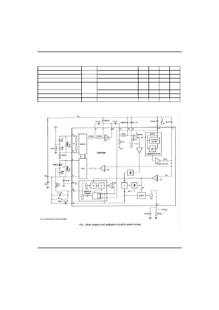
BLOCK DIAGRAM
UTC TDA7088
LINEAR INTEGRATED CIRCUIT
UTC
UNISONIC TECHNOLOGIES CO., LTD.
3
QW-R110-016,A
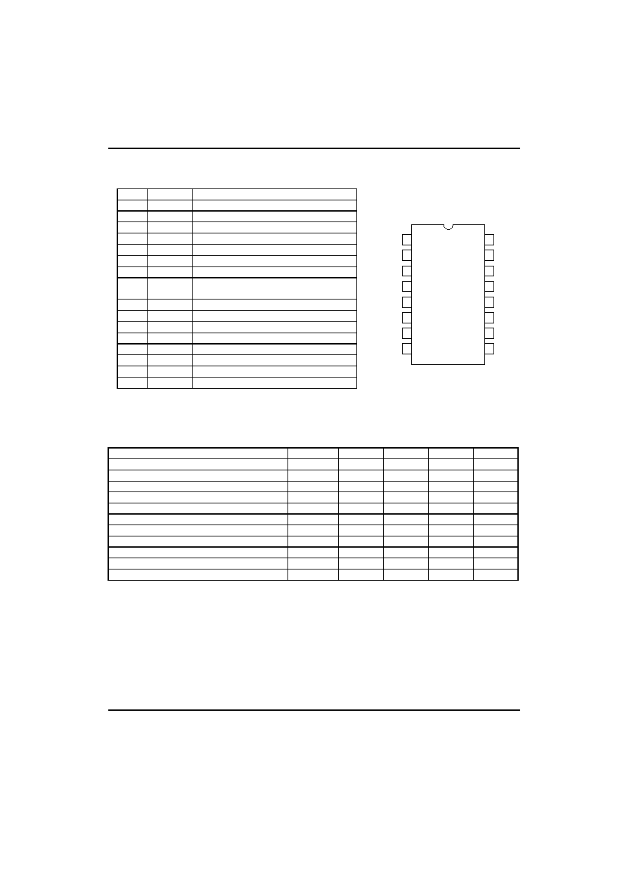
PIN CONFIGURATIONS
Fig.2
DC CHARACTERISTICS
Vp=3V,Tamb=25
∞
C, unless otherwise specified.
PARAMETER
SYMBOL
MIN
TYP
MAX
UNIT
Supply Voltage (pin4)
Vp
1.8
3
5
V
Supply Current (pin4)
Ip
4.2
5.2
6.6
mA
DC voltage on pin1
V1
2.5
2.55
2.6
V
DC voltage on pin3
V3
2.64
2.69
2.74
V
DC voltage on pins 6 and 7
V6,7
2.38
2.44
2.5
V
DC voltage on pin 8
V8
1.6
1.67
1.74
V
DC voltage on pin 9,10 and 13
V9,10,13
2.42
2.47
2.52
V
DC voltage on pins 11 and 12
V11,12
0.91
0.94
0.98
V
DC voltage on pin 15
V15
2.06
2.12
2.18
V
AF output current on pin2
I2
45
60
80
µ
A
Oscillator current on pin5
I5
275
375
500
µ
A
1
2
3
4
5
6
7
8
9
10
11
12
13
14
15
16
MUTE
V
OAF
LOOP
V
P
OSC
IFFB
C
LP1
V
OIF
V
iIF
C
LP2
V
iRF
C
LIM
V
iRF
GND
C
AP
TUNE
TDA7088
PIN
SYMBOL
DESCRIPTION
1
MUTE
Mute output
2
V
OAF
Audio frequency output signal
3
LOOP
AF loop filter
4
V
P
+3V supply voltage
5
OSC
Oscillator resonant circuit
6
IFFB
IF feedback
7
C
LP1
Low-pass capacitor of 1 dB amplifier
8
V
OIF
IF output to external coupling capacitor (high-
pass)
9
V
iLF
IF input to limiter amplifier
10
C
LP2
Low-pass capacitor of IF limiter amplifier
11
V
iRF
Radio frequency input
12
C
iRF
Radio frequency input
13
C
LIM
Limiter offset voltage capacitor
14
GND
Ground(0V)
15
C
AP
All-pass filter capacitor/input for search tuning
16
TUNE
Electrical tuning/AFC output
UTC TDA7088
LINEAR INTEGRATED CIRCUIT
UTC
UNISONIC TECHNOLOGIES CO., LTD.
4
QW-R110-016,A
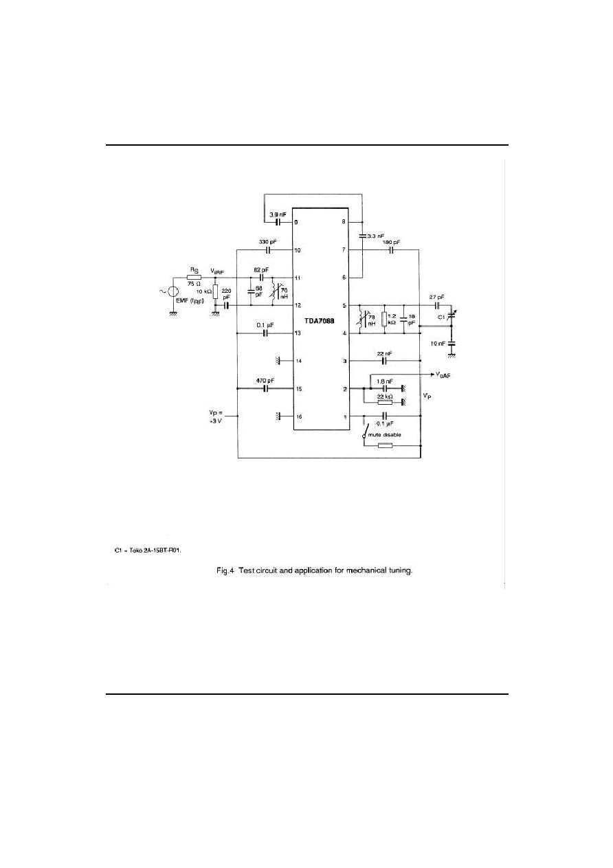
AC CHARACTERISTICS
Vp=3V,Tamb=25
∞
C, fiRF=96MHz modulated with fmod=1kHz and +-22.5kHz deviation; Vi=400
µ
V(measured as
EMF,Rs=75
) and measurements taken in Fig.4;unless otherwise specified.
PARAMETER
SYMBOL
CONDITIONS
MIN
TYP
MAX
UNIT
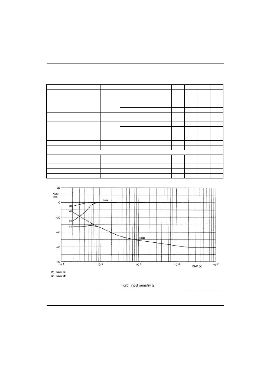
RF sensitivity input voltage (RMS
value)
Vi(rms)
V
OAF
=-3dB;V
OAF
=0dB at
Vi=1mV;see Fig.3
Mute off
Mute on
3
3
6
6
12
µ
V
µ
V
(S+N)/N =26dB
5
10
µ
V
Signal handling
Vi(rms)
f=+-75kHz,THD<10%
100
200
mV
Signal plus noise-to-noise ratio
(S+N)/N
See Fig.3
52
56
dB
Total harmonic distortion
THD
f=+-22.5kHz
1
1.4
%
f=+-75kHz
2.4
3.3
%
AM suppression
AM
FM:1kHz,+-75kHz,
AM:1kHz,m=0.8
47
52
dB
Ripple rejection
RR1000
100mV RMS ripple on Vp,f=1kHz
7
10
dB
Audio output signal (RMS value)
Vo(rms)
RL=22k
60
85
120
mV
Search Tuning (with BB910 and C16=0.1
µ
F) see Fig.1
Minimum output voltage on pin16
V16
Limiting point
Vp -
1.85
V
Tuning steepness
V/
t
Voltage at pin16
95
210
420
mV/s
Oscillator steepness
F
osc
/
t
1.25
2.83
5.6
MHz/s
AFC steepness
I
AFC
/
V3
Voltage at pin3
4.75
9.5
19
µ
S
UTC TDA7088
LINEAR INTEGRATED CIRCUIT
UTC
UNISONIC TECHNOLOGIES CO., LTD.
5
QW-R110-016,A
TEST CIRCUIT