UTC TEA1062/1062A LINEAR INTEGRATED CIRCUIT
UTC
UNISONIC TECHNOLOGIES CO., LTD.
1
QW-R108-001,A
LOW VOLTAGE TELEPHONE
TRANSMISSION CIRCUIT WITH
DIALLER INTERFACE
DESCRIPTION
The UTC TEA1062/1062A is a bipolar integrated
circuit performing all speech and line interface
function, required in the fully electronic
telephone sets. It performs electronic switching
between dialing speech. The circuit is able to
operate down to D.C. line voltage of 1.6V (with
reduced performance) to facilitate the use of more
telephone sets in parallel.
FEATURES
* Low d.c. line voltage; operates down to 1.6V
(excluding polarity guard).
*Voltage regulator with adjustment static resistance.
*Provides supply with limited current for external
circuitry.
*Symmetrical high-impedance inputs (64k
)for
dynamic, magnetic or piezoelectric microphones.
*Asymmetrical high-impedance inputs (32k
)for
electret microphones.
*DTMF signal input with confidence tone.
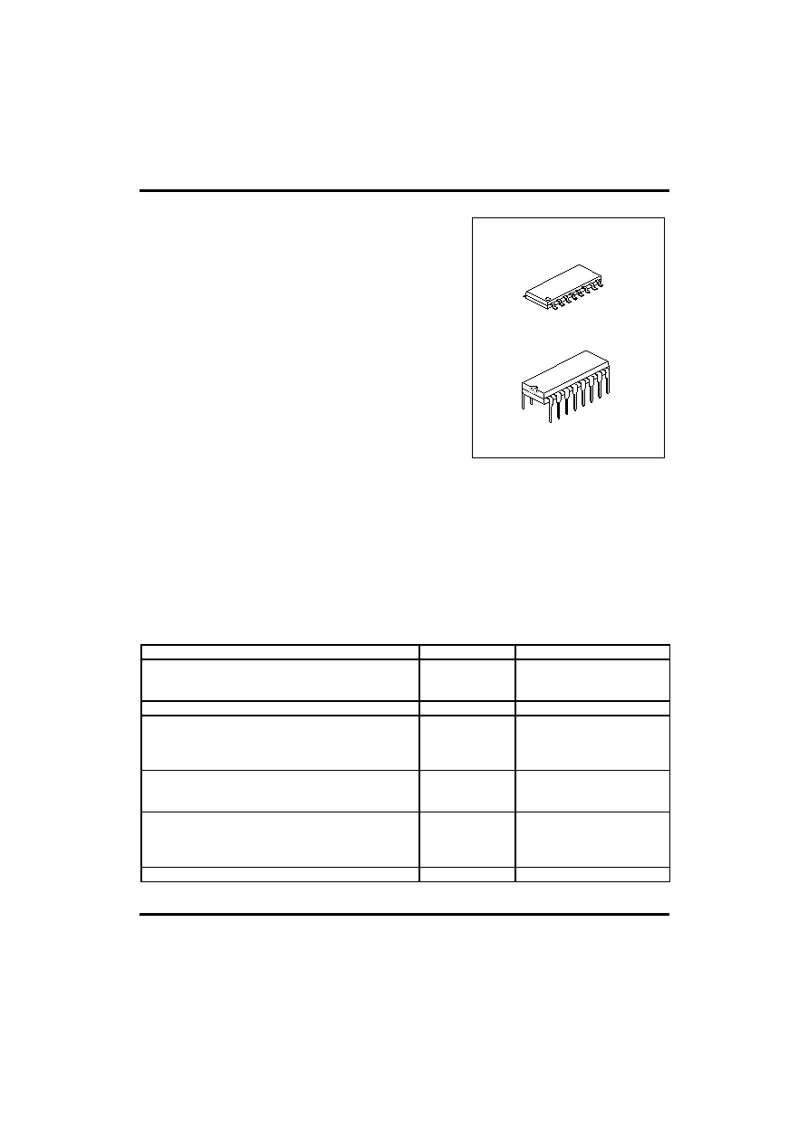
DIP-16
SOP-16
*Mute input for pulse or DTMF dialing.
*Receivering amplifier for several types of earphones.
*Large amplification setting range on microphone
and earpiece amplifiers.
*Line loss compensation facility , line current
depedant (microphone and earpiece amplifiers).
*Gain control adaptable to exchange supply.
*Possibility to adjust the d.c. line voltage.
QUICK REFERENCE DATA
Line voltage at I
line
=15mA
V
LN
typ. 3.8 V
Line current operating range[pin1]
normal operation
with reduced performance
I
line
I
line
11 to 140 mA
1 to 11 mA
Internal supply current
I
CC
typ. 1mA
Supply current for peripherials
at I
line
=15 mA MUTE input LOW(1062 is HIGH)
VCC>2.2V
VCC>2.8V
I
p
I
p
typ. 1.8mA
typ. 0.7mA
Voltage amplification range
microphone amplifier
receiving amplififer
A
VD
A
VD
44 to 52 dB
20 to 39 dB
Line loss compansation
Amplification control range
Exchange supply voltage range
Exchange feeding bridge resistance range
A
VD
V
exch
R
exch
typ. 6 dB
36 to 60V
400 to 1000
Operating ambient temperature range
T
amb
-25 to +75
∞
C

UTC TEA1062/1062A LINEAR INTEGRATED CIRCUIT
UTC
UNISONIC TECHNOLOGIES CO., LTD.
2
QW-R108-001,A
dB
SUPPLY AND
REFERENCE
CONTROL
CURRENT
CURRENT
REFERENCE
LOW
VOLTAGE
CIRCUIT
2
3
16
8
15
14
9
12
11
6
7
10
13
1
5
4
REG
AGC
V
EE
MUTE
DTMF
MIC-
MIC+
IR
V
CC
LN
GAR
QR
GAS1
GAS2
SLPE
STAB
Fig.1 Block Diagram
1 LN positive line terminal
2 GAS1 gain adjustment; transmitting amplifier
3 GAS2 gain adjustment; transmitting amplifier
4 QR non-inverting output,receiving amplifier
5 GAR gain adjustment; receiving amplifier
6 MIC- inverting microphone input
7 MIC+ on-inverting microphone input
8 STAB current stabilizer
9 VEE negative line terminal
10 IR receiving amplifier input
11 DTMF dual-tone multi-frequency input
12 MUTE mute input
13 Vcc positive supply decoupling
14 REG voltage regulator decoupling
15 AGC automatic gain control input
16 SLPE slope (DC resistance) adjustment
Fig.2 PIN CONFIGURATIONS
1
2
3
4
5
6
7
8
16
15
14
13
12
11
10
9
LN
GAS1
GAS2
QR
GAR
MIC-
MIC+
STAB
V
EE
IR
DTMF
MUTE
V
CC
REG
AGC
SLPE
UTC TEA1062/1062A LINEAR INTEGRATED CIRCUIT
UTC
UNISONIC TECHNOLOGIES CO., LTD.
3
QW-R108-001,A
ABSOLUTE MAXIMUM RATINGS
PARAMETER TEST
CONDITIONS SYMBOL
MIN
MAX
UNIT
Positive Continuous Line Voltage
VLN
12
V
Repetitive Line Voltage During
Switch-On Or Line Interruption
VLN
13.2
V
Repetitive Peak Line Voltage for a 1 ms Pulse/5s
R10=13
R9=20
(see
Fig.15)
VLN
28
V
Line Current (1)
R9=20
Iline 140
mA
Voltage on All Other Pins
Vi
VCC+0.7
V
-Vi
0.7
V
Total Power Dissipation(2)
R9=20
Ptot 640
mW
Storage Temperature Range
Tstg
-40
+125
∞
C
Operating Ambient Temperature Range
Tamb
-25
+75
∞
C
Junction Temperature
Tj
+125
∞
C
1. Mostly dependent on the maximum required T
amb
and the voltage between LN and SLPE (see Figs 6 ).
2. Calculated for the maximum ambient temperature specified T
amb
=75
∞
C and a maximum junction temperature of
125
∞
C.
THERMAL RESISTANCE
From junction to ambient in free air Rth j-a = 75K/W
ELECTRICAL CHARACTERISTICS
(Iline=11 to 140mA;V
EE
=0V;f=800Hz;T
amb
=25
∞
C; unless otherwise
specified)
PARAMETER TEST
CONDITIONS
SYMBOL
MIN
TYP
MAX
UNIT
Supply; LN and VCC(pins 1 and 13)
Voltage Drop Over Circuit,
between LN and V
EE
MIC inputs open
I
line
=1mA V
LN
1.6
V
I
line
=4mA V
LN
1.9
V
I
line
=15mA V
LN
3.55
4.0
4.25 V
I
line
=100mA V
LN
4.9
5.7
6.5 V
I
line
=140mA V
LN
7.5
V
Variation with Temperature
I
line
=15mA
V
LN
/
T
-0.3
mV/K
Voltage Drop Over Circuit,
between LN and VEE with
External Resistor R
VA
I
line
=15mA
R
VA
(LN to REG)
=68k
3.5
V
I
line
=15mA
R
VA
(REG to SLPE)
=39k
4.5
V
Supply Current
V
CC
=2.8V I
CC
0.9 1.35 mA
Supply Voltage Available for
Peripheral Circuitry
I
line
=15mA
TEA1062
I
p
=1.2mA;MUTE=HIGH V
CC
2.2
2.7
V
l
p
=0mA;MUTE=HIGH V
CC
3.4
V
TEA1062A
I
p
=1.2mA;MUTE=LOW V
CC
2.2
2.7
V
l
p
=0mA;MUTE=LOW V
CC
3.4
V
UTC TEA1062/1062A LINEAR INTEGRATED CIRCUIT
UTC
UNISONIC TECHNOLOGIES CO., LTD.
4
QW-R108-001,A
ELECTRICAL CHARACTERISTICS
(continued)
PARAMETER TEST
CONDITIONS
SYMBOL
MIN
TYP
MAX
UNIT
Microphone inputs MIC+ and MIC- (pins 6 and 7)
Input impedance (differential)
between MIC- and MIC+
Z
i
64
k
Input impedance (sigle-ended)
MIC- or MIC+ to V
EE
Z
i
32
k
Common Mode Rejection Ratio
k
CMR
82
dB
Voltage Gain
MIC+ or MIC- to LN
I
line
=15mA
R7=68k
G
v
50.5
52.0 53.5
dB
Gain Variation with Frequency
at f=300Hz and f=3400Hz
w.r.t.800Hz
G
vf
+-0.2
dB
Gain Variation with Temperature
at -25
∞
C and +75
∞
C
w.r.t.25
∞
C
without
R6;
I
line
=50mA
G
vT
+-0.2
dB
Dual-tone multi-frequency
input DTMF (pin 11)
Input impedance
Z
i
20.7 k
Voltage Gain from DTMF to LN
I
line
=15mA
R7=68k
G
v
24
25.5
27
dB
Gain Variation with Frequency
at f=300Hz and f=3400Hz
w.r.t.800Hz
G
vf
+-0.2 dB
Gain Variation with Temperature
at -25
∞
C and +75
∞
C
w.r.t.25
∞
C
I
line
=50mA
G
vT
+-0.2 dB
Gain Adjustment GAS1 and GAS2 (pins 2 and 3)
Gain Variation of the Transmitting
Amplifier by Varying R7 between
GAS1 and GAS2
G
v
-8 0 dB
Sending Amplifier Output LN(pin 1)
Output Voltage
I
line
=15mA
THD=10%
V
LN
(rms)
1.7 2.3 V
I
line
=4mA
THD=10%
V
LN
(rms)
0.8 V
Noise output voltage
I
line
=15mA;
R7=68k
;
200
between
MIC- and MIC+;
psophometrically
weighted
V
NO
(rms)
-69
dBmp
Receiving Amplifier Input IR (pin 10)
Input impedance
Z
i
21 k
Receiving Amplifier Output QR (pin 4)
Output Impedance
Z
o
4
Voltage gain from IR to QR
I
line
=15mA;
R
L
(from pin 9 to
pin 4 )=300
G
v
29.5
31
32.5
dB
UTC TEA1062/1062A LINEAR INTEGRATED CIRCUIT
UTC
UNISONIC TECHNOLOGIES CO., LTD.
5
QW-R108-001,A
ELECTRICAL CHARACTERISTICS
(continued)
PARAMETER TEST
CONDITIONS
SYMBOL
MIN
TYP
MAX
UNIT
Gain Variation with Frequency
at f=300Hz and f=3400Hz
w.r.t.800Hz
G
vf
±
0.2
dB
Gain Variation with Temperature
at-25
∞
C and +75
∞
C
w.r.t.25
∞
C
without R6
I
line
=50mA
G
vT
+-0.2 dB
Output Voltage
sinwave drive;
I
p
=0mA;THD=2%
R4=100k
I
line
=15mA
R
L
=150
V
O
(rms)
0.22
0.33 V
R
L
=450
V
O
(rms)
0.3 0.48
V
Output Voltage
THD=10%
R4=100k
R
L
=150
I
line
=4mA V
O
(rms)
15 mV
Noise Output Voltage
I
line
=15mA
R4=100k
IR
open-circuit
psophometrically
weighted
RL=300
V
NO
(rms)
50
µ
V
Gain adjustment GAR (pin 5)
Gain Variation of Receiving
Amplifier Achievable by
Varying
R4 between GAR and QR
G
v
-11
0
dB
Mute Input (pin 12)
Input Voltage(HIGH)
V
IH
1.5 V
CC
V
Input Voltage(LOW)
V
IL
0.3
V
Input Current
I
MUTE
8 15
µ
A
Reduction of Gain
MIC+ or MIC- to QR
MUTE=LOW
G
v
70 dB
Voltage Gain from DTMF to QR
MUTE=LOW
R4=100k
RL=300
G
v
-19 dB
Automatic Gain Control Input AGC
(
pin 15)
Controlling the Gain from lR to QR
and the Gain from MIC+/MIC-
to LN;R6 between AGC and VEE R6=110k
Gain Control Range
I
line
=70mA
G
v
-5.8
dB
Highest Line Current
for Maximum Gain
I
line
23
mA
Minimum Line Current
for Minimum Gain
I
line
61
mA

UTC TEA1062/1062A LINEAR INTEGRATED CIRCUIT
UTC
UNISONIC TECHNOLOGIES CO., LTD.
6
QW-R108-001,A
FUNCTIONAL DESCRIPTION
Supply: VCC, LN, SLPE, REG and STAB
Power for the UTC TEA1062/1062A and its
peripheral circuits is usually obtained from the
telephone line. The IC supply voltage is derived from
the line via a dropping resistor and regulated by the
UTC TEA1062/1062A,The supply voltage Vcc may
also be used to supply external circuits e.g. dialling and
control circuits. Decoupling of the supply voltage is
performed by a capacitor between Vcc and V
EE
while the internal voltage regulator is decoupled by a
capacitor between REG and V
EE.
The DC current
drawn by the device will vary in accordance with
varying values of the exchange voltage(V
exch
), the
feeding bridge resistance(R
exch
) and the DC resistance
of the telephone line(R
line
). The UTC
TEA1062/1062A has an internal current stabilizer
operating at a level determined by a 3.6k resistor
connected between STAB and VEE( see Fig.8).
When the line current(I
line
) is more than 0.5 mA greater
than the sum of the IC supply current ( Icc) and the
current drawn by the peripheral circuitry connected to
V
CC
(l
p
) the excess current is shunted to V
EE
via LN.
The regulated voltage on the line terminal(V
LN
) can be
calculated as:
V
LN
=V
ref
+I
SLPE
*R9 or;
V
LN
=V
ref
+[(I
line ≠
I
CC -
0.5*10-
3
A)I
p
]*R9
where:V
ref
is an internally generated temperature
compensated reference voltage of 3.7V and R9 is an
external resistor connected between SLPE and V
EE
. In
normal use the value of R9 would be 20
. Changing
the value of R9 will also affect microphone gain, DTMF
gain,gain control characteristics, side tone level,
maxmimum output swing on LN and the DC
characteristics (especially at the lower voltages). Under
normal conditions, when I
SLPE>=
I
CC
+0.5mA +I
p
, the
static behaviour of the circuit is that of a 3.7V regulator
diode with an internal resistance equal to that of
R9.In the audio frequency range the dynamic
impedance is largely determined by R1.Fig.3 shows
the equivalent impedance of the circuit.
Microphone inputs(MIC+ and MIC-) and
gain pins (GAS1 and GAS2)
The UTC TEA1062/1062A has symmetrical inputs.
Its input impedance is 64k
(2*32k
) and its voltage
gain is typically 52 dB (when R7=68k
.see Fig.13).
Dynamic, magnetic, piezoelectric or electret (with
built-in FET source followers) can be used. Microphone
arrangements are illustrated in Fig.10. The gain of the
microphone amplifier can be adjusted between 44dB
and 52dB to suit the sensitivity of the transducer in use.
The gain is proportional to the value of R7 which is
connected between GAS1 and GAS2. Stability is
ensured by the external capacitors, C6 connected
between GAS1 and SLPE and C8 connected between
GAS1 and VEE. The value of C6 is 100pF but this
may be increased to obtain a first-order low-pass filter.
The value of C8 is 10 times the value of C6. The cut-off
frequency corresponds to the time constant R7*C6.
Mute input (MUTE)
A LOW(UTC TEA1062 is HIGH) level at MUTE
enables DTMF input and inhibites the microphone
inputs and the receiving amplifier inputs; a HIGH(UTC
TEA1062 is LOW) level or an open circuit does the
reverse. Switching the mute input will cause negligible
clickis at the telephone outputs and on the line. In case
the line current drops below 6mA(parallal opration of
more sets) the circuit is always in speech condition
independant of the DC level applied to the MUTE input.
Dual-tone multi-frequency input (DTMF)
When the DTMF input is enabled dialling tones may
be sent onto the line. The voltage gain from DTMF to
LN is typically 25.5dB(when R7=68k
) and varies with
R7 in the same way as the microphone gain. The
signalling tones can be heard in the earpiece at a low
level(confidence tone).
Receiving amplifier (IR,QR and GAR)
The receiving amplifier has one input (IR) and a
non-inverting output (QR). Earpiece arrangements are
illustrated in Fig.11. The IR to QR gain is typically 31dB
(when R4=100k
). It can be adjusted between 20 and
31dB to match the sensitivity of the transducer in use.
The gain is set with the value of R4 which is connected
between GAR and QR.The overall receive gain,
between LN and QR, is calculated by substracting the
anti-sidetone network attenuation (32dB) from the
amplifier gain. Two external capacitors, C4 and C7,
ensure stability. C4 is normally 100pF and C7 is 10
times the value of C4. The value of C4 may be
increased to obtain a first-order low-pass filter.The
cut-off frequency will depend on the time constant
R4*C4. The output voltage of the receiving amplifier is
specified for continuous-wave drive. The maximum
output voltage will be higher under speech conditions
where the peak to RMS ratio is higher.

UTC TEA1062/1062A LINEAR INTEGRATED CIRCUIT
UTC
UNISONIC TECHNOLOGIES CO., LTD.
7
QW-R108-001,A
Automatic gain control input(AGC)
Automatic line loss compensation is achieved by
connecting a resistor(R6) between AGC and V
EE
. The
automatic gain control varies the gain of the
microphone amplifier and the receiving amplifier in
accordance with the DC line current. The control range
is 5.8dB which corresponds to a line length of 5km for
a 0.5mm diameter twisted pair copper cable with a DC
resistance of 176
/km and average attenuation of
1.2dB/km. Resistor R6 should be chosen inaccordance
with the exchange supply voltage and its feeding
bridge resistance(see Fig.12 and Table 1). The ratio of
start and stop currents of the AGC curve is
independent of the value of R6. If no automatic line
loss compensation is required the AGC may be left
open-circuit. The amplifier, in this condition, will give
their maximum specified gain.
Side-tone suppression
The anti-sidetone network, R1//Z
line
, R2, R3, R8, R9
and Z
bal
,(see Fig.4) suppresses the transmitted signal
in the earpiece. Compensation is maximum when the
following conditions are fulfilled:
(a) R9*R2=R1[R3+(R8//Z
bal
)];
(b) [Z
bal
/(Z
bal
+R8)]=[Z
line
/(Z
line
+R1)];
If fixed values are chosen for R1, R2, R3 and R9 then
condition(a) will always be fullfilled when R8/Z
bal
lR3.
To obtain optimum side-tone suppression condition(b)
has to be fulfilled which results in:
Z
bal
=(R8/R1) Z
line
=k*Z
line
where k is a scale factor;
K=(R8/R1).
The scale factor (k), dependent on the value of R8,
is chosen to meet following criteria:
(a) Compatibility with a standard capacitor from the
E6 or E12 range for Z
bal,
(b)Z
bal
//R8R3 fulfilling condition (a) and thus
ensuring correct anti-sidetone bridge operation,
(c) Z
bal
+R8R9 to avoid influencing the trans-
mitter gain.
In practice Z
line
varies considerably with the type and
length. The value chosen for Z
bal
should therefore be
for an average line length thus giving optimum setting
for short or long lines.
Example
The balance impedance Z
bal
at which the optimum
suppression is present can be calculated by: Suppose
Z
line
= 210
+(1265
//140nF) representing a 5km line
of 0.5 mm diameter, copper, twisted pair cable
matched to 600
(176
/km;38nF/km). When k=0.64
then R8=390
,Z
bal
=130
+(820
//220nF). At line
currents below 9mA the internal reference voltage is
automatically adjusted to a lower value(typically 1.6V
at 1mA) This means that more sets can be operated in
parallel with DC line voltages (excluding the polarity
guard) down to an absolute minimum voltage of 1.6V.
With line currents below 9mA the circuit has limited
sending and receiving levels. The internal reference
voltage can be adjusted by means of an external
resistor(R
VA
). This resistor when connected between
LN and REG will decrease the internal reference
voltage and when connected between REG and SLPE
will increase the internal reference voltage. Current(I
p
)
available from V
CC
for peripheral circuits depends on
the external components used. Fig.9 shows this
current for V
CC
>
2.2V. If MUTE is LOW (1062 is
HIGH)when the receiving amplifier is driven the
available current is further reduced. Current availability
can be increased by connecting the supply IC(1081)
in parallel with R1, as shown in Fig.16(c), or, by
increasing the DC line voltage by means of an
external resistor(R
VA
) connected between REG and
SLPE.

UTC TEA1062/1062A LINEAR INTEGRATED CIRCUIT
UTC
UNISONIC TECHNOLOGIES CO., LTD.
8
QW-R108-001,A
LN
V
EE
Leq
Vref
Rp
R1
C3
C1
100
µ
F
4.7
µ
F
REG
V
CC
R9
20
Rp=16.2k
Leq=C3*R9*Rp
Fig.3 Equivalent impedance circuit
The anti-sidetone network for the UTCTEA1062/1062A family shown in Fig.4 attenuates the signl received from
the line by 32 dB before it enters the receiving amplifier. The attenuation is almost constant over the whole audio
frequency range. Fig.5 shows a convertional Wheatstone bridge anti-sidetone circuit that can be used as an
alternative. Both bridge types can be used with either resistive or complex set impedances.
Zline
R1
R9
R2
R3
R8
Zbal
Rt
IR
V
EE
SLPE
i
m
Fig 4 Equivalent circuit of UTC TEA1062/1062A
anti-sidetone bridge
Zline
R1
R9
R2
R8
Rt
IR
V
EE
SLPE
i
m
R
A
Fig 5 Equivalent circuit of an anti-sidetone
network in a wheatstone bridge
configuration
UTC TEA1062/1062A LINEAR INTEGRATED CIRCUIT
UTC
UNISONIC TECHNOLOGIES CO., LTD.
9
QW-R108-001,A
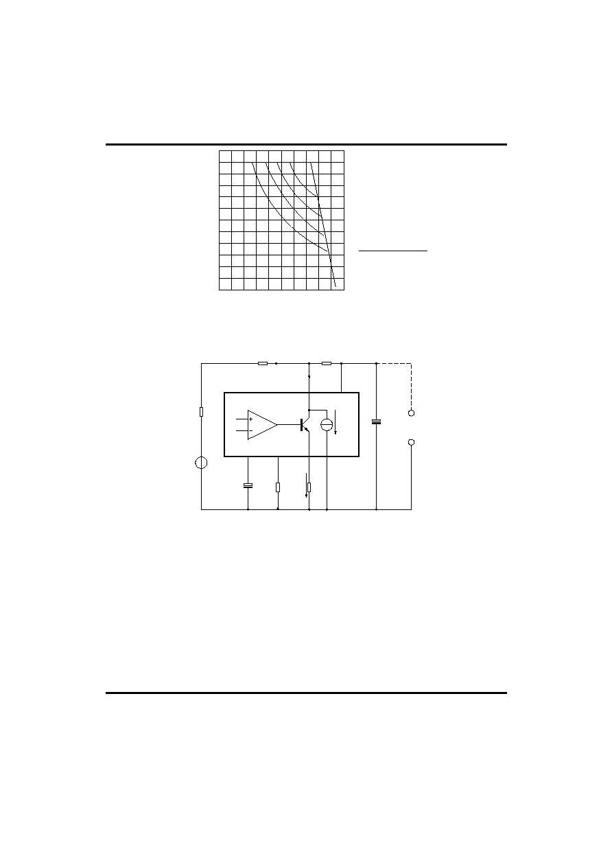
150
130
110
90
70
50
30
2
4
6
8
10
12
(1)
(2)
(3)
(4)
V
LN
-V
SLPE
(V)
I
line
(mA)
(1) 45∞C 1068mW
(2) 55∞C 934mW
(3) 65∞C 800mW
(4) 75∞C 666mW
Tamb
Ptot
Fig.6 UTC TEA1062/ TEA1062A safe operating area
Fig.8 Supply arrangement
DC
AC
REG
STAB
SLPE
V
EE
V
CC
LN
Rexch
Vexch
Rline
I
line
R1
C3
R5
R9
C1
PERIPHERAL
CIRCUITS
0.5mA
I
SLPE
I
SLPE
0.5mA
+
UTC TEA1062/1062A LINEAR INTEGRATED CIRCUIT
UTC
UNISONIC TECHNOLOGIES CO., LTD.
10
QW-R108-001,A
Fig.9 Typical current Ip available from Vcc peripheral circuitry with Vcc>=2.2V.
curve (a) is valid when the receiving amplifier is not driven or when MUTE =LOW
(UTC TEA1062 is
HIGH)
.curve(b) is valid when MUTE=HIGH
(UTC TEA1062 is LOW)
and the receiving amplifier is
driven;Vo(rms)=150mV,R
L
=150
.The supply possibilities can be increased simply by setting the voltage drop
over the circuit V
LN
to a high value by means of resistor R
VA
connected between REG and SLPE.
7
6
MIC+
MIC-
(1)
7
6
MIC+
MIC-
V
EE
V
CC
13
9
7
6
MIC-
MIC+
(a)
(b)
(c)
Fig. 10 Alternative microphone arrangement
(a) Magnetic or dynamic microphone. The resistor marked(1) may be connected to decrease the terminating
impedance.
(b) Electret microphone.
(c) Piezoelectric microphone.
0
0.8
1.6
2.4
I
p
(mA)
0
1
2
3
4
5
a
b
V
cc(V)
(a) Ip=2.1mA
(b) Ip=1.7mA
Iline=15mA at V
LN
=4V
R1=620
and R9=20
UTC TEA1062/1062A LINEAR INTEGRATED CIRCUIT
UTC
UNISONIC TECHNOLOGIES CO., LTD.
11
QW-R108-001,A
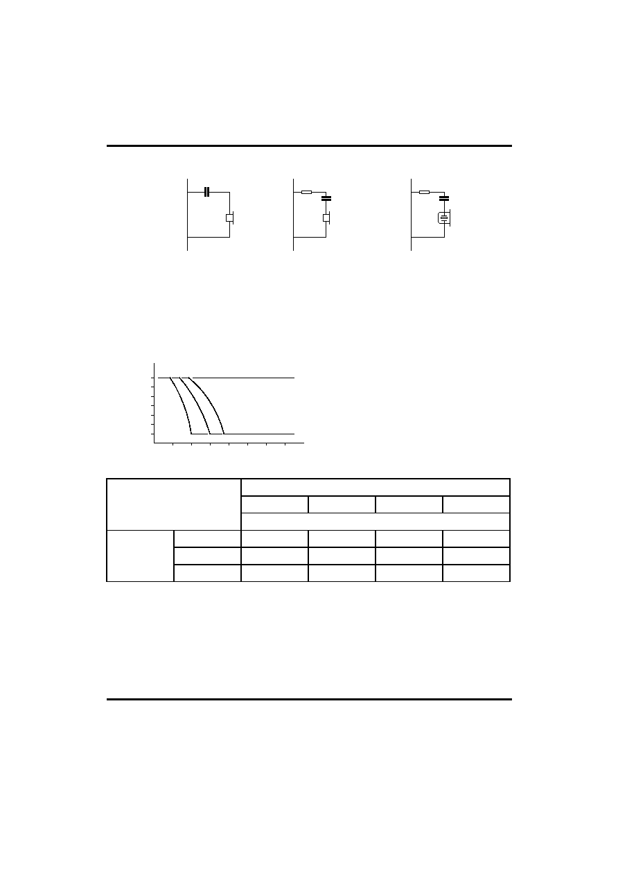
(a) Dynamic earpiece.
(b) Magnetic earpiece.The resistor marked(1) may be connected to prvent distortion(inductive load)
(c) Piezoelectric earpiece.The earpiece marked(2) is requirred to increase the phase margin (capacitive load)
Fig.12 Variation of gain with line urrent,with R6 as a parameter.
Rexch(
)
400
600
800 1000
R6(k
)
36
100
78.7
◊
◊
Vexch(V)
48 140 110 93.1 82
60 ◊
◊
120 102
Table 1 Values of resistor R6 for optimum line loss compensation,for various usual values of exchange
supply vloltage(Vexch) and exchange feeding bridge resistance(Rexch);R9=20
.
4
9
QR
V
EE
9
4
QR
V
EE
4
9
QR
V
EE
(2)
(1)
(a)
(b)
(c)
Fig.11 Alternative receiver arrangement
-6
-4
-2
0
0
20
40
60
80
100
120
140
Iline (mA)
Gv
(dB)
R6=
R9=20
78.7k
110k
140k
(1) (2) (3)
(3)
(1)
(2)
R6=
R6=
R6=
UTC TEA1062/1062A LINEAR INTEGRATED CIRCUIT
UTC
UNISONIC TECHNOLOGIES CO., LTD.
12
QW-R108-001,A
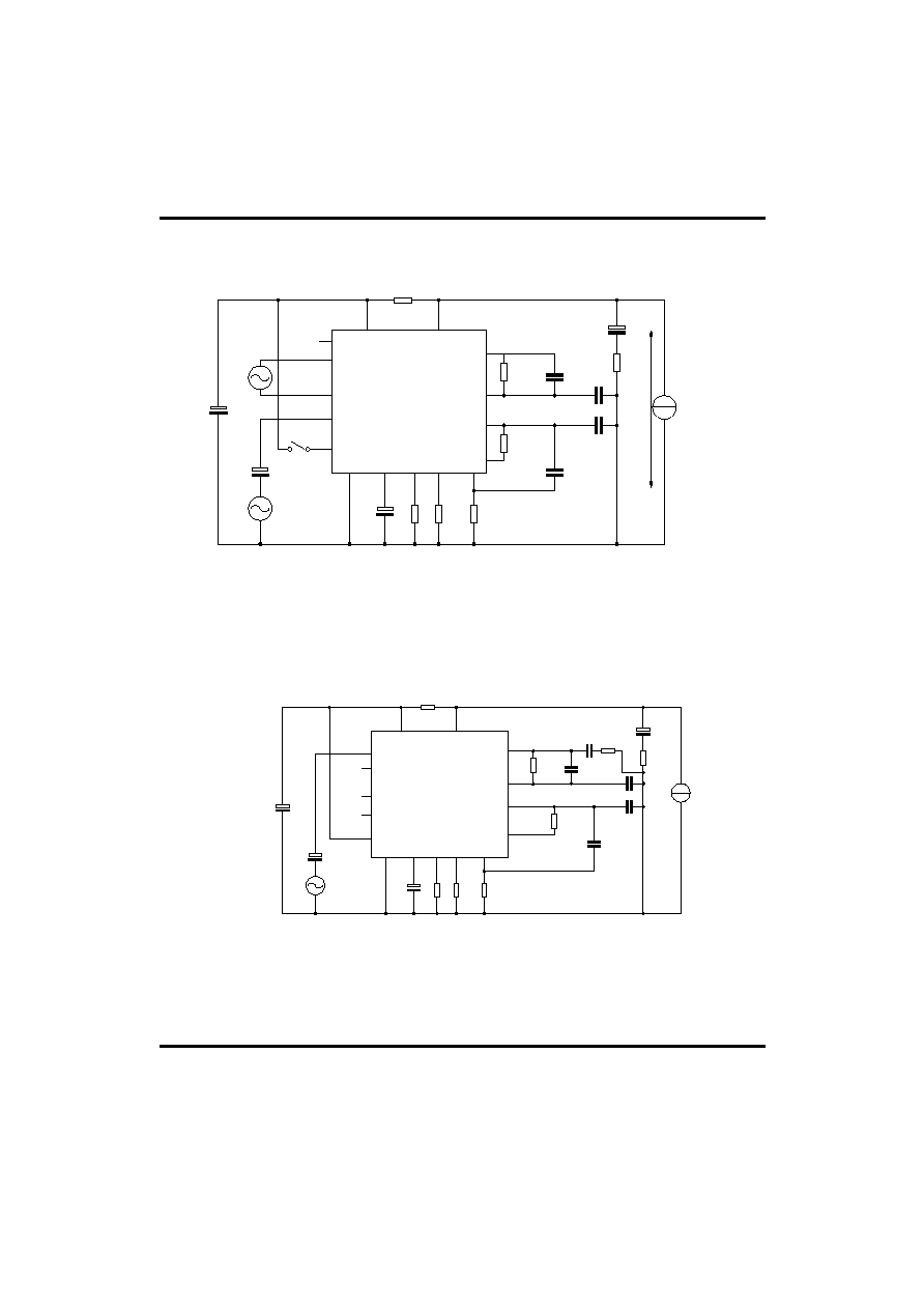
Fig.13 Test circuit defining voltage gain of MIC+,MIC- and DTMF inputs.
Voltage gain is defined as : GV=20*log(|VO/Vi|).For measuring the gain from MIC+ and MIC- the MUTE input
should be HIGH(UTC TEA1062 is LOW) or open-circuit, for measuring the DTMF input MUTE should be
LOW(UTC TEA1062 is HIGH) .Inputs not under test should be open-circuit.
Fig.14 Test circuit for defining voltage gain of the receiving amplifier.
Voltage gain is defined as: GV=20*log(|VO/Vi|).
10
6
11
7
12
13
1
4
5
2
3
16
8
15
14
9
MIC-
MIC+
REG AGC STAB SLPE
GAS2
GAS1
GAR
QR
LN
VCC
VEE
IR
DTMF
MUTE
R1 620
100
µ
F
C4
100pF
C7 1nF
C6
100pF
R4
100k
R7
68k
R9
20
R5
3.6k
R6
C3
4.7
µ
F
10
µ
F
C1
100
µ
F
Vi
Vi
R
L
600
C8 1nF
10 TO 140 mA
Vo
10
6
11
7
12
13
1
4
5
2
3
16
8
15
14
9
MIC-
MIC+
REG AGC STAB
SLPE
GAS2
GAS1
GAR
QR
LN
VCC
VEE
IR
DTMF
MUTE
R1=620
100
µ
F
C4
100pF
C7 1nF
C6
100pF
R4
100k
R7
68k
R9
20
R5
3.6k
R6
C3
4.7
µ
F
10
µ
F
C1
100
µ
F
Vi
600
C8 1nF
10 TO 140 mA
Vo
Z
L
C2
UTC TEA1062/1062A LINEAR INTEGRATED CIRCUIT
UTC
UNISONIC TECHNOLOGIES CO., LTD.
13
QW-R108-001,A
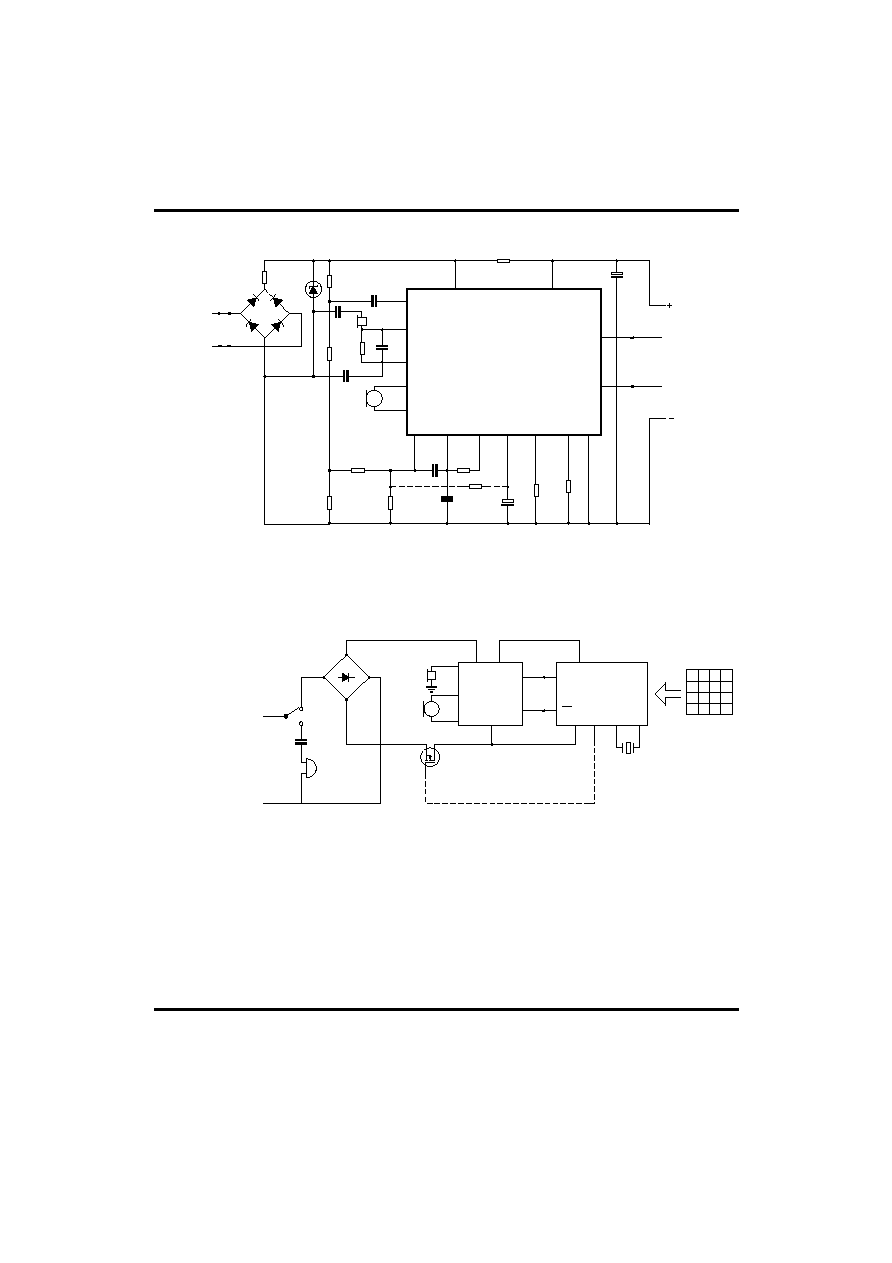
Fig.15 Typical application of the UTC TEA1062A ,shown here with a piezoelectric earpiece and DTMF dialling. The
bridge to the left ,the Zener diode and R10 limit the current into the circuit and the voltage across the circuit during
line transients.Pulse dialling or register recall required a different protection arrangement.
The DC line voltage can be set to a higher value by resistor RVA(REG to SLPE).
VEE
DTMF
MUTE
LN
VCC
DTMF
VSS DP/FL
VDD
M1
CARDLE
CONTRAT
TELEPHONE
LINE
BSN254A
UTC1062A
dialling
circuit
Fig.16 Typical applications of the UTC TEA1062/1062A (simplified)
The dashed lines show an optional flash ( register recall by timed loop break).
SLPE
GAS1
GAS2
REG
AGC
STAB V
EE
DTMF
V
CC
LN
IR
QR
GAR
MIC-
MIC+
MUTE
Telephone
Line
From dial and
control circuits
C1
100
µ
F
13
11
12
10
9
8
7
6
5
4
3
2
1
16
14
15
R1
620
R2
132k
BZX79
C12
R10
130
BAS11
(x2)
BZW14
(x2)
C5
100nF
C2
R4
R3
3.92k
C4
100pF
C7
1nF
R8
390
Zbal
R9
20
C6
100pF
R7
C8
1nF
R
VA
(R16.R14)
C3
4.7
µ
F
R6
R5
3.6k
UTC TEAI062/A