
UTC UC3842A / 3843A
LINEAR INTEGRATED CIRCUIT
UTC
UNISONIC TECHNOLOGIES CO., LTD.
1
QW-R103-002,A
CURRENT MODE PWM CONTROL
CIRCUITS
DESCRIPTION
The UTC UC3842A/3843A provide the necessary functions
to implement off-line or DC to DC fixed frequency current
mode , controlled switching circuits with a minimal external
part count
FEATURES
*Low external part count.
*Low start up current ( Typical 0.12mA )
*Automatic feed forward compensation
*Pulse-by-Pulse current limiting
*Under-voltage lockout with hysteresis
*Double pulse Suppression
*High current totem pole output to drive MOSFET directly
*Internally trimmed band gap reference
*500kHz operation
DIP-8
SOP-8
BLOCK DIAGRAM
7
5
7
6
5
4
3
1
2
8
Internal
Bias
5V REF
S/R
U.V.L.O
R
S
PWM
LATCH
Vref
Good
Logic
ERROR
AMPLIFIER
1/2Vref
1/3Vref
1V
OSCILLATOR
Vref
VFB
COMP
CURRENT SENSE
RT/CT
Vcc
GND
OUTPUT
Vcc
GND
CURRENT
SENSE
COMPARATOR
ABSOLUTE MAXIMUM RATINGS
(Ta=25
∞C)
PARAMETER SYMBOL
VALUE
UNIT
Supply Voltage(Low Impedance Source)
V
CC
30
V
Supply Voltage(Icc<30mA)
Vcc
Self Limiting
V
Output Current ( Peak )
Io
+-1
A
Output Energy(capacity Load)
5
µJ
Analog Inputs(pin 2,3)
V
I(ANA)
-0.3 ~ +6.3
V
Error Amplifier Output Sink Current
I
SINK(EA)
10 mA
Power Dissipation
PD DIP-8
at T
amb
<=25
∞C 1.0
W
SOP-8
at T
amb
<=25
∞C 0.5
W
Lead Temperature( Soldering 10 Sec )
Tlead
300
∞C
UTC UC3842A / 3843A
LINEAR INTEGRATED CIRCUIT
UTC
UNISONIC TECHNOLOGIES CO., LTD.
2
QW-R103-002,A
(continued)
PARAMETRER SYMBOL
VALUE
UNIT
Storage Temperature
Tstg
-65 ~ +150
∞C
Note 1: Ta>25
∞C, P
D
derated with 8mW/
∞C.
ELECTRICAL CHARACTERISTICS
(0
∞C <=Ta<=70∞C,V
CC
=15V,R
T
=10k
,C
T
=3.3nF,unless otherwise
specified)
PARAMETER SYMBOL
TEST
CONDITIONS MIN
TYP
MAX
UNIT
Reference Section
Output Voltage
V
REF
Tj=25
∞C,Io=1mA
4.9
5 5.1 V
Line Regulation
V
REF
12<=V
IN
<=25V
6
20
mV
Load Regulation
V
REF
1<=Io=20mA
6
25
mV
Temperature Stability
(Note 2)
0.2
0.4
mV/
∞C
Total Output Variation
Line, Load, Temp(note 2)
4.82
5.18
V
Output Noise Voltage
Vosc
10Hz<=f<=10kHz,Tj=25
∞C (note 2)
50 uV
Long Term Stability
Ta=25
∞C,1000Hrs(note 2)
5
25
mV
Output Short Circuit
I
SC
-30
-100
-180
mA
Oscillator Section
Initial Accuracy
f
Tj=25
∞C
47 52 57 kHz
Voltage Stability
f/Vcc
12<=Vcc<=25V
0.2
1
%
Temperature Stability
Tmin<=T
A
<=Tmax(note 2)
5
%
Amplitude
Vosc
Vpin 4 peak to peak
1.7
V
Error Amplifier Section
Input Voltage
V
I(EA)
Vpin
1=2.5V 2.42
2.50
2.58
V
Input Bias Current
I
BIAS
-0.3
-2
µA
A
VOL
2
<=Vo<=4V
60
90
dB
Unity Gain Bandwidth
Tj=25
∞C (note 2)
0.7
1
MHz
PSRR
I2<=Vcc<=25V
60
70
dB
Output Sink Current
Isink
Vpin 2=2.7V,Vpin 1=1.1V
2
6
mA
Output Source Current
Isource
Vpin 2=2.3V,Vpin 1=5V
-0.5
-0.8
mA
Vout High
V
OH
Vpin 2=2.3V, RL=15k
to GND
5 6 V
Vout Low
V
OL
Vpin 2=2.7V,Vpin 1=1.1V
0.7
1.1
V
Current Sense section
Gain G
V
(note
3,4)
2.85
3
3.15
V/V
Maximum Input signal
V
I(MAX)
Vpin 1=5V( note 3)
0.9
1
1.1
V
PSRR
12<=Vcc<=25V
70 dB
Input Bias Current
I
BIAS
-2
-10
µA
Delay to Output
Vpin 3=0 to 2V
150
300
ns
Output Section
Output Low Level
V
OL
Isink=20mA
0.1
0.4
V
Isink=200mA
1.5
2.2
V
Output High Level
V
OH
Isource=20mA 13
13.5
V
Isource=200mA
12
13.5
V
Rise Time
t
R
Tj=25
∞C,C
L
=1nF(note 2)
50
150
ns
Fall Time
t
F
Tj=25
∞C,C
L
=1nF(note 2)
50
150
ns
Under-Voltage Lockout Output Section
Start Threshold
V
TH(ST)
UTC3842A 14.5
16
17.5
V
UTC3843A
7.8
8.4
9
V
Min. Operating Voltage
V
OPR(min)
After Turn On
UTC3842A
8.5
10 11.5
UTC3843A
7
7.6
8.2
V
PWM Section
Maximum Duty Cycle
D
(MAX)
95
97
100
%

UTC UC3842A / 3843A
LINEAR INTEGRATED CIRCUIT
UTC
UNISONIC TECHNOLOGIES CO., LTD.
3
QW-R103-002,A
PARAMETER SYMBOL
TEST
CONDITIONS MIN
TYP
MAX
UNIT
Minimum Duty Cycle
D
(MIN)
0
%
Total Standby Current
Start-up Current
I
ST
0.12 0.3 mA
Operating Supply Current
I
CC(opr)
Vpin 2=Vpin 3=0V
11
17
mA
Vcc Zener Voltage
Vz
Icc=25mA
34
V
note 2:These parameters, although guaranteed ,are not 100% tested in production.
note 3:Parameters measured at trip point of latch with Vpin 2=0.
note 4:Gain defined as:
Vpin 1
Vpin 3
A=
; 0<=Vpin3<=0.8V
note 5:Adjust Vcc above the start threshold before setting at 15V.
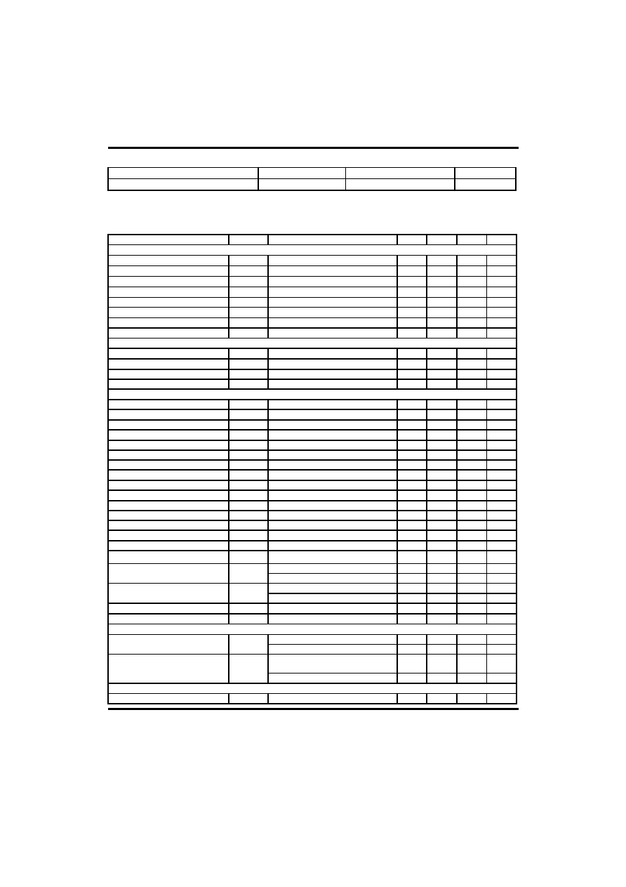
OPEN-LOOP LABORATORY TEST FIXTURE
1
2
8
7
3
6
4
5
A
Vref
Vcc
1k
/ 1W
0.
1
µ
F
CT
RT
100k
5k
4.
7k
4.
7k
0.
1
µ
F
Error Amp
Adjust
I
s
ens
e
Adj
u
s
t
OUTPUT
High peak current associated with capacity loads necessitate careful grounding techniques. Timing and bypass
capacitors should be connected close to pin 5 in single point GND. The transistor and 5k
potentio-meter are used
to sample the oscillator waveform and apply an adjustable Ramp to Pin 3.
UNDER-VOLTAGE LOCKOUT
7
Vcc
Von=16V
Voff=10V
ON/OFF Command
to rest of IC
Von
Voff
<1mA
<15mA
Icc
Vcc
During Under-Voltage Lockout, the output driver is biased to a high impedance state. Pin 6 should be shunt to
GND with a bleeder resistor to prevent activating the power switch with output leakage currents.
UTC UC3842A / 3843A LINEAR INTEGRATED CIRCUIT
UTC
UNISONIC TECHNOLOGIES CO. LTD
4
QW-R103-002,A
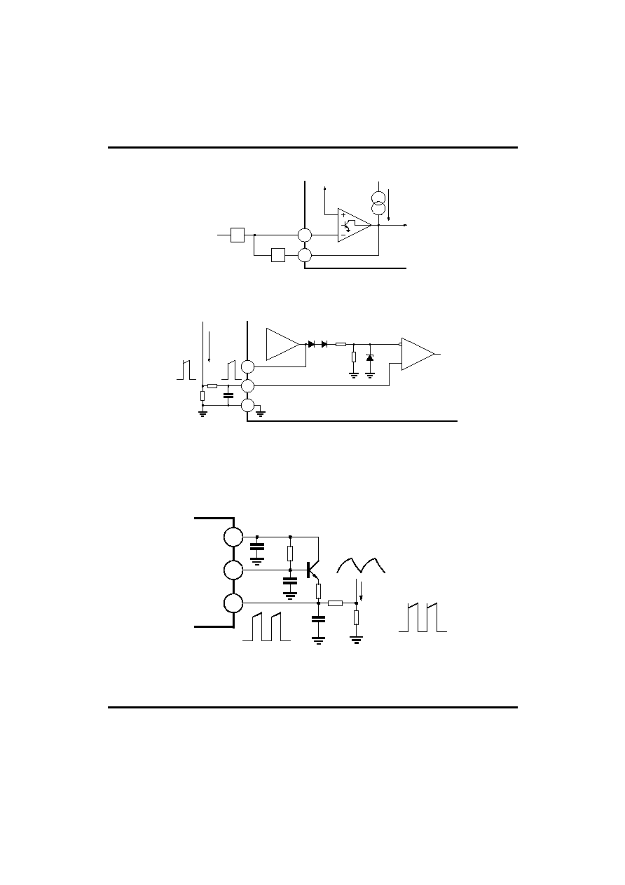
ERROR AMPLIFIER CONFIGURATION
2
1
0.5mA
2.5V
Zf
Zi
Error amplifier can source or sink up to 0.5mA
CURRENT SENSE CIRCUIT
5
3
1
2R
R
1V
C
Rs
R
Is
Error
Amplifier
Current Sense
Comparator
Peak current (Is) determined by the formula:
Ismax=10V/Rs.
A small RC filter be required to suppress switch transients.
SLOPE COMPENSATION
8
4
3
Isense
R1
R2
Rsense
C
RT
CT
0.1
µ
F
A fraction of the oscillator ramp can be resistively summed with the current sense signal to provide slope
compensation for converts requiring duty cycles over 50%.Note that capacitor C, forms a filter with R2 to suppress
the leading edge switch spikes.
UTC UC3842A / 3843A
LINEAR INTEGRATED CIRCUIT
UTC
UNISONIC TECHNOLOGIES CO. LTD
5
QW-R103-002,A
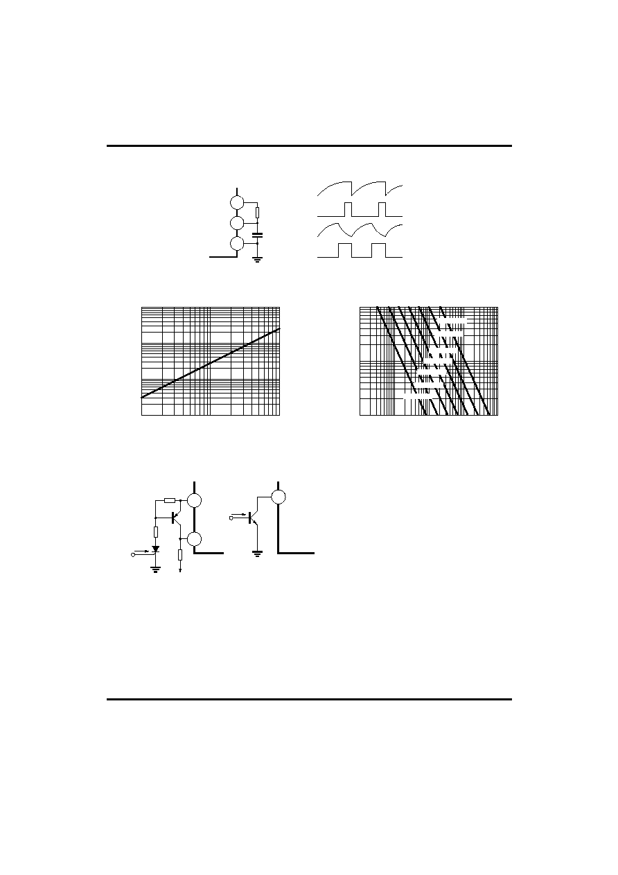
OSCILLATOR SECTION
5
4
8
RT
CT
Large RT
Small CT
Small RT
Large CT
V4
V4
INTERNAL
CLOCK
INTERNAL
CLOCK
Dead time VS C
T
(R
T
>5k
) Timing Resistance Vs Frequency
1
10
100
1
10
100
0.1
td (
µs)
CT (nF)
100
1
10
6
10
5
10
4
10
3
10
10
2
RT (k
)
Frequency (Hz)
CT=1nF
CT=2.2nF
CT=4.7nF
CT=10nF
CT=22nF
CT=47nF
CT=100nF
SHUTDOWN TECHNIQUES
8
3
330
500
1k
1
Shutdown
To current
Sense resistor
Shutdown
Shutdown UTC UC3842A can be
accomplished by two methods; either raise pin 3
above 1V or pull Pin 1 below a voltage two diode
drops above ground. Either method caused the
output of PWM comparator to be high(refer to
block diagram).The PWM latch is reset dominant
so that the output will remain low until the next
clock cycle after the shutdown condition at pins 1
and/or 3 is removed . In one example, an
externally latched shut ≠down may be
accomplished by adding an SCR which be reset
by cycling Vcc below the lower UVLO threshold.
At this point the reference turns off allowing the
SCR to reset.