UTC UR133/A
LINEAR INTEGRATED CIRCUIT
UTC
UNISONIC TECHNOLOGIES CO., LTD.
1
QW-R102-005,I
300/500mA LOW DROPOUT
LINEAR VOLTAGE REGULATOR
DESCRIPTION
The UTC UR133/A is a 300/500mA fixed output
voltage low dropout linear regulator. Wide range of
available output voltage fits most of applications.
Built-in output current-limiting most thermal-limiting
provide maximal protection against any fault
conditions.
FEATURES
*Guaranteed 300/500mA output current
*Input voltage range up to 12V
*Extremely tight load regulation
*Fast transient response
*Current-limiting and Thermal-limiting
*Three-terminal adjustable or fixed 1.5V, 1.8V,2.2V,
2.5V, 2.7V , 2.8V , 2.9V ,3.0V, 3.3V , 3.5V , 3.7V ,
4.7V , 5.0V
APPLICATIONS
*Voltage regulator for LAN Card, CD-ROM, and DVD
*Wireless communication systems
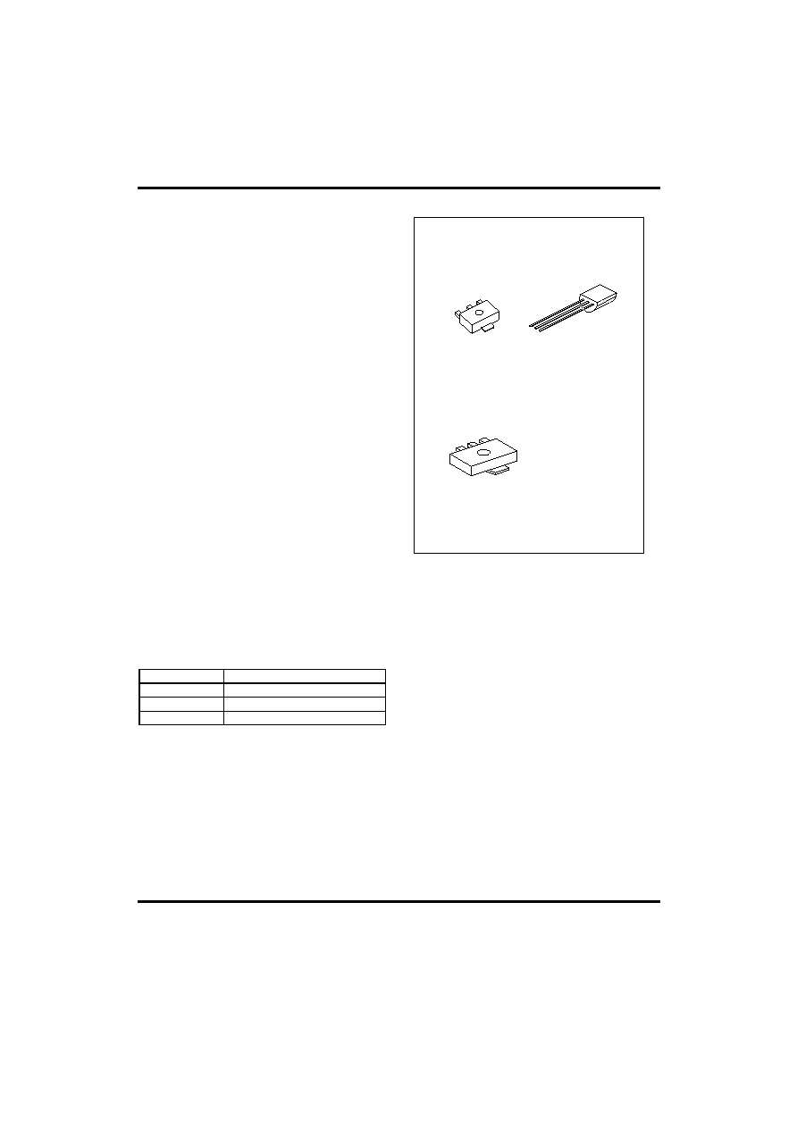
SOT-223
TO-92
1
SOT-89
1
3
2 1
PIN DESCRIPTION
NAME FUNCTION
VOUT Output
GND Ground/Adjustable
VIN
Positive Power Input

UTC UR133/A
LINEAR INTEGRATED CIRCUIT
UTC
UNISONIC TECHNOLOGIES CO., LTD.
2
QW-R102-005,I
MARKING INFORMATION
PACKAGE VOLTAGE
CODE
PIN CODE PIN 1 PIN 2 PIN 3
MARKING
A GND
OUT
IN
B OUT
GND
IN
C GND
IN
OUT
SOT-89
D IN
GND
OUT
1
2
3
R133/A
DATE
CODE
PIN CODE
VOLTAGE
CODE
A GND
OUT
IN
B OUT
GND
IN
C GND
IN
OUT
TO-92
D IN
GND
OUT
1
2
3
UTC
UR133/A
VOLTAGE
CODE
DATE
CODE
PIN CODE
A GND
OUT
IN
B OUT
GND
IN
C GND
IN
OUT
SOT-223
1 5 : 1 . 5 V
1 8 : 1 . 8 V
2 2 : 2 . 2 V
2 5 : 2 . 5 V
2 7 : 2 . 7 V
2 8 : 2 . 8 V
2 9 : 2 . 9 V
3 0 : 3 . 0 V
3 3 : 3 . 3 V
3 5 : 3 . 5 V
3 7 : 3 . 7 V
4 7 : 4 . 7 V
5 0 : 5 . 0 V
A D :
ADJUSTABLE
D IN
GND
OUT
1
2
3
UR133/A
VOLTAGE
CODE
DATE
CODE
PIN CODE
ABSOLUTE MAXIMUM RATINGS
PARAMETER MIN.
TYP.
MAX.
UNIT
Input Voltage Vin
-0.3
12
V
Operating Junction Temperature Range
-40
125
�C
Storage Temperature Range
-65
150
�C
Power Dissipation
SOT-89
Thermal Resistance, R
OJC
=100
�C/W
Thermal Resistance, R
OJA
=300
�C/W
TO-92
Thermal Resistance, R
OJA
=160
�C/W
SOT-223
Thermal Resistance, R
OJC
=15
�C/W
Thermal Resistance R
OJA
=60
�C/W (est)
0.50
0.60
0.80
W

UTC UR133/A
LINEAR INTEGRATED CIRCUIT
UTC
UNISONIC TECHNOLOGIES CO., LTD.
3
QW-R102-005,I
UTC UR133/A 1.5V, 1.8V, 2.2V, 2.5V, 2.7V, 2.8V, 2.9V,3.0V
ELECTRICAL CHARACTERISTICS
(Ta=25
�C, C
IN
=1
�F, C
OUT
=10
�F, unless otherwise specified)
PARAMETER TEST
CONDITIONS
MIN
TYP.
MAX
UNITS
Output Voltage UR133/A
I
L
=1mA, V
IN-
V
OUT
=1.4V 1.47
1.77
2.16
2.45
2.65
2.74
2.84
2.94
1.50
1.80
2.20
2.50
2.70
2.80
2.90
3.00
1.53
1.83
2.24
2.55
2.75
2.86
2.96
3.06
V
Output Voltage Temperature
Coefficient
50
150
PPM/
�C
Line Regulation
I
L
=1mA, V
IN-
Vout=2V~Vin=9V
0.5
%V
OUT
Load Regulation
(note 2)
UR133
UR133A
I
L
=1mA~300mA, V
IN-
Vout =2V
I
L
=1mA~500mA, V
IN-
Vout =2V
10
10
30
50
mV
mV
Current Limit (note 3)
UR133
UR133A
V
IN-Vout
=2V, V
OUT
=0V
350
550
mA
mA
Dropout Voltage (note 4,5)
1.5
V
Standby current
I
L
=0, V
IN
=9V
3.0
mA
UTC UR133/A ADJ 3.3V, 3.5V, 3.7V, 4.7V, 5.0V
ELECTRICAL CHARACTERISTICS
(Ta=25
�C, C
IN
=1
�F, C
OUT
=10
�F, unless otherwise specified)
PARAMETER TEST
CONDITIONS
MIN
TYP.
MAX
UNITS
Adjustable (R1=120,R2=200,Vout=3.3V)
Reference Voltage
Vin-Vo=2V, I
L
=1mA 1.238
1.250
1.262
V
Output Voltage UR133/A
I
L
=1mA, V
IN-
V
OUT
=1.4V 3.23
3.43
3.63
4.61
4.90
3.30
3.50
3.70
4.70
5.00
3.37
3.57
3.77
4.79
5.10
V
Output Voltage Temperature
Coefficient
50
150
PPM/
�C
Line Regulation
I
L
=1mA, V
IN-
Vout=2V~Vin=12V
0.5 %V
OUT
Load Regulation
(note 2)
UR133
UR133A
I
L
=1mA~300mA, V
IN-
Vout =2V
I
L
=1mA~500mA, V
IN-
Vout =2V
10
10
30
50
mV
mV
Current Limit (note 3)
UR133
UR133A
V
IN-Vout
=2V, V
OUT
=0V
350
550
mA
mA
Dropout Voltage (note 4,5)
1.3
V
Standby current
I
L
=0, V
IN
=12V
5.0
mA
Note 1: Guaranteed by design.
Note 2: Regulation is measured at constant junction temperature, using pulsed ON time.
Note 3: Current Limit is measured at constant junction temperature, using pulsed ON time.
Note 4: Dropout is measured at constant junction temperature, using pulsed ON time, and the criterion is V
OUT
inside target value
�2%.
Note 5: Dropout test is skipped at the condition of V
IN
<3V.

UTC UR133/A
LINEAR INTEGRATED CIRCUIT
UTC
UNISONIC TECHNOLOGIES CO., LTD.
4
QW-R102-005,I
TYPICAL APPLICATION CIRCUIT
UTC
UR133/A
APPLICATION INFORMATION
A 10
�F (or larger) capacitor is recommended between V
OUT
and GND for stability. The part may oscillate
without the capacitor. Any type of capacitor can be used, but not Aluminum electrolytics when operating below -25
�C.
The capacitance may be increased without limit.
A 1
�F capacitor (or larger) should be placed between V
IN
to GND.
UR133/A ADJUSTABLE
UTC
UR133/A
+
+
V
REF
R1
R2
10
uF
1
uF
V
OUT
V
IN
10
uF
Cr
Cr:10uF to improve ripple rejection
V
OUT
=V
REF
(1+R2/R1)+I
ADJ
*R2
I
ADJ
+
V
IN
V
OUT
ADJ

UTC UR133/A
LINEAR INTEGRATED CIRCUIT
UTC
UNISONIC TECHNOLOGIES CO., LTD.
5
QW-R102-005,I
UR133
O
u
t
p
u
t
C
u
rren
t, I
OU
T
(
mA
)
4
5
6
7
8
0
100
200
9 10
250
300
Input Voltage (V)
11 12
3
50
150
13
V
OUT
=5.0V
V
OUT
=4.7V
V
OUT
=3.7V
V
OUT
=3.5V
V
OUT
=3.3V
V
OUT
=2.5V
Output Current v.s. Input Voltage
Ground Current vs.Input Voltage
Input Voltage (V)
G
r
ou
nd
C
u
r
r
e
nt (
m
A
)
0
2
4
6
8
0
1
2
3
4
10
12
V
OUT
=1.5V,1.8V,2.2V,2.5V,
2.7V,2.8V,2.9V,3.0V
V
OUT
=4.7V,5.0V
V
OUT
=3.3V,3.5V,3.7V
Dropout Voltage vs.Load Current
Load Current (mA)
D
r
op
ou
t V
o
ltag
e
(
V
)
0
50
100
150
200
0
1.2
1.3
1.4
1.5
250
300
1.6
1.7
V
OUT
=1.5V,1.8V,2.2V,2.5V,2.7V,
V
OUT
=4.7V,5.0V
V
OUT
=3.3V,3.5V,3.7V
Line Transient Response
I
n
put
V
o
l
t
ag
e(
V
)
0 0.1 0.2 0.3 0.4
6
8
-50
0
0.5 0.6
50
100
Time (mS)
0.7
Ou
t
p
u
t
V
o
l
t
a
g
e
(m
V,AC)
0.8 0.9 1.0
I
L
=1mA
V
OUT
=5.2V
C
OUT
=1uF
Load Transient Response
Lo
ad
C
u
r
r
e
nt
(m
A)
0 0.5 1.0 1.5 2.0
0.1
150
-60
-40
2.5 3.0
-20
0
Time (mS)
3.5
Ou
t
p
u
t
V
o
l
t
a
g
e
(m
V,AC
)
4.0 4.5 5.0
20
Load Transient Response
Lo
ad C
u
r
r
e
n
t
(m
A)
0 0.5 1.0 1.5 2.0
0.1
150
-40
2.5 3.0
-20
0
Time (mS)
3.5
O
u
t
put
V
o
l
t
age
(m
V,
AC
)
4.0 4.5 5.0
20
V
OUT
=5.2V
C
OUT
=1uF
40
2.8V,2.9V,3.0V

UTC UR133/A
LINEAR INTEGRATED CIRCUIT
UTC
UNISONIC TECHNOLOGIES CO., LTD.
6
QW-R102-005,I
UR133A
O
u
tpu
t
C
u
r
r
e
n
t, I
OU
T
(
mA
)
4
5
6
7
8
0
100
200
9 10
250
300
Input Voltage (V)
11 12
3
50
150
13
V
OUT
=4.7V
V
OUT
=3.7V
V
OUT
=3.5V
V
OUT
=3.3V
V
OUT
=2.5V
350
400
450
500
V
OUT
=5.0V
Output Current v.s. Input Voltage
Ground Current vs.Input Voltage
Input Voltage (V)
G
r
ound
C
u
r
r
ent
(
m
A
)
0
2
4
6
8
0
1
2
3
4
10
12
V
OUT
=4.7V,5.0V
V
OUT
=3.3V,3.5V,3.7V
5
6
V
OUT
=1.5V,1.8V,2.2V,2.5V,2.7V,
Dropout Voltage vs.Load Current
Load Current (mA)
D
r
opou
t
V
o
l
t
age (
V
)
0
50 100 150 200
0
1.2
1.3
1.4
1.5
250300
1.6
1.7
500
450
400
350
V
OUT
=1.5V,1.8V,2.2V,2.5V,2.7V,
V
OUT
=4.7V,5.0V
V
OUT
=3.3V,3.5V,3.7V
Load Transient Response
Load
C
u
r
r
ent
(m
A
)
0 0.2 0.4 0.6 0.8
0.1
250
-40
-20
1.0 1.2
0
20
Time (mS)
1.4 1.6 1.8 2.0
40
V
OUT
=5.0V
C
OUT
=1uF(Tantalum)
O
u
t
put
V
o
lt
a
g
e
(m
V,AC
)
Load Transient Response
L
oad C
u
r
r
e
n
t
(m
A
)
0 0.2 0.4 0.6 0.8
0.1
250
-40
-20
1.0 1.2
0
20
Time (mS)
1.4
O
u
t
p
ut
V
o
l
t
age
(m
V
,
AC)
1.6 1.8 2.0
40
V
OUT
=5.0V
C
OUT
=1uF(Tantalum)
Line Regulation Response
I
n
p
u
t
V
o
l
t
age(
V
)
0 0.1 0.2 0.3 0.4
6
8
-50
0
0.5 0.6
50
100
Time (mS)
0.7
O
u
t
put
V
o
lt
age
(
m
V,AC
)
0.8 0.9 1.0
I
L
=1mA
V
OUT
=5.0V
C
OUT
=1uF(Tantalum)
2.8V,
2.9V,
3.0V
2.8V,2.9V,3.0V