UTC BT138
TRIAC
UTC
UNISONIC TECHNOLOGIES CO., LTD.
1
QW-R401-002,A
TRIACS LOGIC LEVEL
DESCRIPTION
Passivated triacs in a plastic envelope, intended for use in
applications requiring high bidirectional transient and blocking
voltage capability and high thermal cycling performance. Typical
applications include motor control, industrial and domestic
lighting, heating voltages and static switching
.
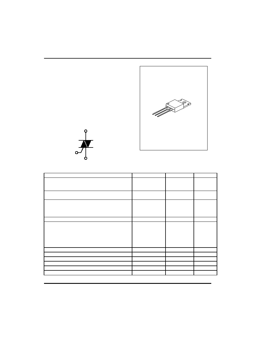
SYMBOL
MT2
MT1
G
TO-220
1
1:MT1 2:MT2 3:GATE
ABSOLUTE MAXIMUM RATINGS
( Tj=25
�C)
PARAMETER SYMBOL
RATING
UNIT
Repetitive Peak Off State Voltage
BT138-600
BT138-800
V
DRM
600
800
V
RMS On-state Current
(Full sine wave; Tmb99
�C)
I
T(RMS)
12 A
Non-repetitive Peak. On-State Current
(Full sine wave; Tj=25
�C prior to surge)
t=20ms
t=16.7ms
I
TSM
95
105
A
I
2
t For Fusing (t=10ms)
I
2
t 45
A
2
s
Repetitive Rate of Rise of On-state Current after Triggering
(I
TM
=20A;I
G
=0.2A; dI
G
/dt=0.2A/
�s)
T2+G+
T2+G-
T2-G-
T2-G+
dI
T
/dt
50
50
50
10
A/
�s
Peak Gate Voltage
V
GM
5
V
Peak Gate Current
I
GM
2
A
Peak Gate Power
P
GM
5
W
Average Gate Power
P
G(AV)
0.5
W
Operating Junction Temperature
Tj
125
�C
Storage Temperature
Tstg
-40~150
�C
UTC BT138
TRIAC
UTC
UNISONIC TECHNOLOGIES CO., LTD.
2
QW-R401-002,A
*Although not recommended, off-state voltages up to 800V may be applied without damage, but the triac may switch
to the on-state. The rate of rise of current should not exceed 15A/
�s.
THERMAL RESISTANCES
PARAMETER SYMBOL
MIN
TYP
MAX
UNIT
Thermal Resistance, Junction to Mounting Base
Full cycle
Half cycle
Rj-mb
1.5
2.0
�C /W
Thermal Resistance, Junciton to Ambient
In free air
Rj-a
60 -
�C /W
STATIC CHARACTERISTICS
(Tj=25
�C,unless otherwise specified)
PARAMETER SYMBOL
TEST
CONDITIONS
MIN
TYP
MAX
UNIT
Gate Trigger Current
T2+G+
T2+G-
T2-G-
T2-G+
I
GT
V
D
=12V, I
T
=0.1A
5
8
10
12
35
35
35
70
mA
Latching Current
T2+G+
T2+G-
T2-G-
T2-G+
I
L
V
D
=12V, I
GT
=0.1A
7
20
8
10
40
60
40
60
mA
Holding Current
I
H
V
D
=12V, I
GT
=0.1A
6
30
mA
On-State Voltage
V
T
I
T
=15A
1.4
1.65
V
Gate Trigger Voltage
V
GT
V
D
=12V, I
T
=0.1A
V
D
=400V, I
T
=0.1A, Tj=125
�C
0.25
0.7
0.4
1.5
V
Off-state Leakage Current
I
D
V
D
=V
DRM(max)
, Tj=125�C
0.1 0.5 mA
DYNAMIC CHARACTERISTICS
(Tj=25
�C,unless otherwise specified)
PARAMETER SYMBOL
TEST
CONDITIONS
MIN
TYP
MAX
UNIT
Critical Rate Of Rise Of Off-State
Voltage
dV
D
/dt V
DM
=67% V
DRM(max)
, Tj=125
�C
Exponential waveform,
Gate open circuit
100 250 V/
�s
Critical Rate Of Change
Of Commutating Voltage
dV
com
/dt V
DM
=400V,Tj=95
�C, I
T(RMS)
=12A
dl
com
/dt =5.4A/ms,
Gate open circuit
20 V/
�s
Gate Controlled Turn-on Time
tgt
I
TM
=16A, V
D
=V
DRM(max)
,
I
G
=0.1A dI
G
/dt=5A/
�s
2
�s

UTC BT138
TRIAC
UTC
UNISONIC TECHNOLOGIES CO., LTD.
3
QW-R401-002,A
TYPICAL CHARACTERISTICS
1ms
100us
10us
1000
T/s
Figure 2. Maximum Permissible Non-repetitive
Peak On-state Current I
TSM
,vs Pulse W idth
t
p
,for Sinusoidal Currents,t
p
20ms
10
100
5
10
0
20
5
IT(RMS)/A
Figure 1.Maximum on -state Dissipation.Ptot vs RMS
On-state Current,I
T(RMS)
,W here
=conduction Angle.
15
0
15
10
10ms
100ms
100
150
-50
50
0
15
5
Tmb/
10
0
95
117.5
102.5
125
110
Ptot/W
Tmb(max)/C
=180
=120
=90
=60
=30
Figure 4.Maximum Permissible RMS Current I
T(RMS)
vs mounting baseTemperature T
m b
IT(RMS)/A
99
ITSM/A
I
T
I
TSM
time
Tj initial=25
m ax
dI
T
/dt limit
T2-G+ quadrant
25
10
Surge Duration /S
15
20
5
0
Figure 5.Maximum Permissible Repetitive RMS on-state
Current IT(RMS),vs Surge Duration,for Sinusoidal
Currents,f=50Hz;Tmb
99
IT(RMS)/A
0.01
0.1
1
10
100
40
Number of Cycles at 50Hz
80
60
20
0
Figure 3 .Maximum Permissible Non-Repetitive
peak on-state Current I
TSM
,vs Number of Cycles,
for Sinusoidal Currents,f=50Hz
10
100
ITSM/A
1
1000
I
T
time
I
TSM
Tj initial=25
m ax
100
150
-50
50
0
1.6
0.8
Tj/
1.2
1.4
1
0.6
0.4
Figure 6.Normalised Gate Trigger Voltage V
GT
(Tj)/
V
GT
(25
),vs Junction Temperature Tj
V
GT
(25
)
V
GT
(Tj
)
T
T

UTC BT138
TRIAC
UTC
UNISONIC TECHNOLOGIES CO., LTD.
4
QW-R401-002,A
1ms
0.1ms
10us
0.1
tp/s
Figure 11.Transient Thermal Impedance
Zth j-mb,vs Pulse W idth tp
0.001
0.01
10ms
0.1s
1.5
2
0
1
0.5
40
VT/V
30
20
10
0
Figure 10.Typical and Maximum
On-state Characteristic
IT/A
Zth j-mb (K/W )
100
150
-50
50
0
3
1
Tj/
2
2.5
1.5
0.5
0
Figure 7.Normalised Gate Trigger Current
I
GT
(Tj)/I
GT
(25
),vs Junction Temperature Tj
I
GT
(25
)
I
GT
(Tj
)
T2+G+
T2+G-
T2-G-
T1-G+
typ
max
100
150
-50
50
0
3
1
Tj/
2
2.5
1.5
0.5
0
Figure 8.Normalised Latching Current
I
L
(Tj)/I
L
(25
),vs Junction Temperature Tj
I
L
(25
)
I
L
(Tj
)
100
150
-50
50
0
3
1
Tj/
2
2.5
1.5
0.5
0
Figure 9.Normalised Holding Current
I
H
(Tj)/I
H
(25
),vs Junction Temperature Tj
I
H
(25
)
I
H
(Tj
)
1s
10s
1
10
unidirectional
bidirectional
tp
t
P
D
100
150
50
0
1000
10
Tj/
100
1
Figure 12.Typical commutation dV/dt vs junction
temperature,parameter commutation dl
T
/dt.The triac should
commutate when the dV/dt is below the value on the
appropriate curve for pre-commutation dl
T
/dt
dV/dt(V/us)
2.5
3
Tj=125
Tj=25
Vo=1.75V
Rs=0.316Ohms
dIcom/dt=5.4A/ms