
UTRON
UT51C164
Rev 1.5
256K X 16 BIT EDO DRAM
UTRON TECHNOLOGY INC. P90005
1F, No. 11, R&D Rd. II, Science-Based Industrial Park, Hsinchu, Taiwan, R. O. C.
TEL: 886-3-5777882 FAX: 886-3-5777919
1
REVISION HISTORY
REVISION DESCRIPTION Draft
Date
Rev. 1.0 Original.
Apr 30 ,1999
Rev. 1.1 Add 40 pin TSOP-II Package.
Jun 7 ,1999
Rev. 1.2 Add 3.3V range.
Jul 30,1999
Rev. 1.3 Revised Datasheet name to be UT51C164/UT51L164.
Sep 22,2000
Rev. 1.4 1.Separated V
DD
=5V and V
DD
=3.3V version.
2.Revise symbols "RAS#CAS#OE#WE#" to be " RAS CAS
OE
WE
".
Jan 23,2002
Rev. 1.5 1. Add access time 25ns, delete 60ns
2. Add DC/AC characteristics for ≠25ns
Oct 22,2002

UTRON
UT51C164
Rev 1.5
256K X 16 BIT EDO DRAM
UTRON TECHNOLOGY INC.
P90005
1F, No. 11, R&D Rd. II, Science-Based Industrial Park, Hsinchu, Taiwan, R. O. C.
TEL: 886-3-5777882 FAX: 886-3-5777919
2
FEATURES
RAS access time: 25, 35, 40, 50
2 CAS Byte/Word Read/Write operation
CAS - before ≠ RAS refresh capability
RAS only and Hidden refresh capability
Early write or output enable controlled write
Extended Data Out operation
Package : 40 pin 400mil SOJ
40 / 44 pin 400mil TSOP-
Single 5V+10% power supply
TTL compatible inputs and outputs
512 refresh cycles /8ms
Speed
-25 -35 -40 -50
t
RAC
25ns 35ns 40ns 50ns
t
CAA
12ns 18ns 20ns 24ns
t
PC
10ns 14ns 15ns 19ns
t
CAC
7ns 11ns 12ns 14ns
t
RC
45ns 70ns 75ns 90ns
GENERAL DESCRIPTION
The UT51C164 is high speed 5V EDO DRAMs organized as 256K bit X 16 I/O and fabricated with
the CMOS process. The UT51C164 offers a combination of unique features including : EDO Page
Mode operation for higher bandwidth with Page Mode cycle time as short as 14ns. All inputs are
TTL compatible. Input and output capacitance is significantly lowered to increase performance and
minimize loading. These features make the UT51C164 suited for wide variety of high performance
computer systems and peripheral applications
UTRON
UT51C164
Rev 1.5
256K X 16 BIT EDO DRAM
UTRON TECHNOLOGY INC.
P90005
1F, No. 11, R&D Rd. II, Science-Based Industrial Park, Hsinchu, Taiwan, R. O. C.
TEL: 886-3-5777882 FAX: 886-3-5777919
3
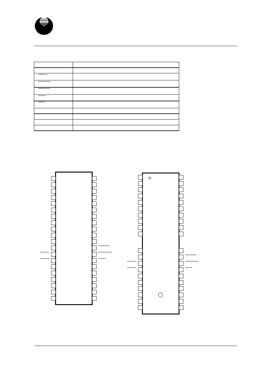
PIN DESCRIPTION
SYMBOL DESCRIPTION
A0-A8 Address
Inputs
RAS
Row Address Strobe
UCAS
Column Address Strobe / Upper Byte Control
LCAS
Column Address Strobe / Lower Byte Control
WE
Write enable
OE
Output enable
DQ0-DQ15
Data Inputs, Data Outputs
V
DD
+5V
Supply
Vss 0V
Supply
NC No
Connect
PIN CONFIGURATIONS
1
2
3
4
5
6
7
8
9
10
11
12
13
14
15
16
17
18
19
20
40
39
38
37
36
35
34
33
32
31
30
29
28
27
26
25
24
23
22
21
V
DD
DQ0
DQ1
DQ2
DQ3
V
DD
DQ4
DQ5
DQ6
DQ7
NC
NC
WE
RAS
NC
A0
A1
A2
A3
V
DD
Vss
DQ15
DQ14
DQ13
DQ12
Vss
DQ11
DQ10
DQ9
DQ8
NC
LCAS
UCAS
OE
A8
A7
A6
A5
A4
Vss
UT51C164
40- pin SOJ
1
2
3
4
5
6
7
8
9
10
11
12
13
14
15
16
17
18
19
20
40
39
38
37
36
35
34
33
32
31
30
29
28
27
26
25
24
23
22
21
V
DD
DQ0
DQ1
DQ2
DQ3
V
DD
DQ4
DQ5
DQ6
DQ7
NC
NC
WE
RAS
NC
A0
A1
A2
A3
V
DD
Vss
DQ15
DQ14
DQ13
DQ12
Vss
DQ11
DQ10
DQ9
DQ8
NC
LCAS
UCAS
OE
A8
A7
A6
A5
A4
Vss
UT51C164
40-pin TSOP II
UTRON
UT51C164
Rev 1.5
256K X 16 BIT EDO DRAM
UTRON TECHNOLOGY INC.
P90005
1F, No. 11, R&D Rd. II, Science-Based Industrial Park, Hsinchu, Taiwan, R. O. C.
TEL: 886-3-5777882 FAX: 886-3-5777919
4
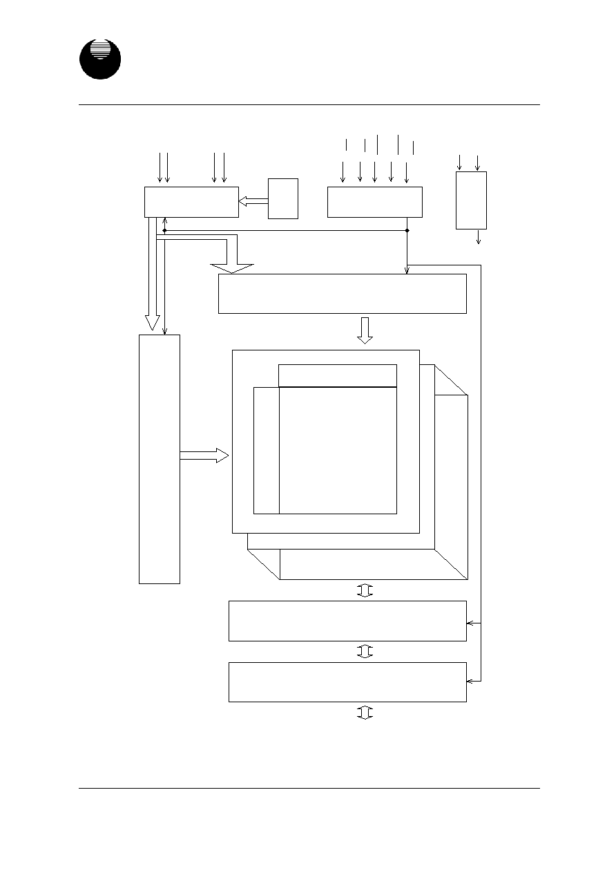
FUNCTION BLOCK DIAGRAM
Column Decoder
Cell Array
512 x 512 x 16
FSA & Write in Circuit
Input & Output Buffer
Row Control Circuit
Control Circuit
V
BB
GENERATOR
Refresh
Counter
Sense
A
mp
Address Buffers
& Predecoders
Row Decoder
V
BB
V
DD
V
SS
A0
A1
.
A7
A8
9
Y0
≠Y
8
X0
≠
X
8
X512 CS
x16
x16
x16
DQ[0,15]
RAS
LCAS
UCAS
WE
OE
..
.

UTRON
UT51C164
Rev 1.5
256K X 16 BIT EDO DRAM
UTRON TECHNOLOGY INC.
P90005
1F, No. 11, R&D Rd. II, Science-Based Industrial Park, Hsinchu, Taiwan, R. O. C.
TEL: 886-3-5777882 FAX: 886-3-5777919
5
ABSOLUTE MAXIMUM RATINGS
PARAMETER SYMBOL
VALUE
UNIT
Voltage on any pin relative to Vss
V
T
-1.0 to +7
V
Supply voltage relative to V
SS
V
DD
-1.0 to +7
V
Short circuit output current
I
OUT
50
mA
Power dissipation
P
D
1.0
W
Operating temperature
T
A
0 to + 70
∫C
Storage temperature
T
STG
-55 to +125
∫C
Notes: Permanent device damage may occur if absolute maximum ratings are exceed.
RECOMMENDED DC OPERATING CONDITIONS
(T
A
= 0 to 70∫C)
5.0V
PARAMETER
SYMBOL
MIN MAX
UNIT
NOTES
V
DD
4.5 5.5
V
1
Supply voltage
Vss 0 0
V
-
Input high voltage
V
IH
2.4
V
DD
+1V
V
1
Input low voltage
V
IL
-0.3
0.8
V
1
Notes: 1. All Voltage referred to Vss
CAPACITANCE
(T
A
= 25∫C, V
DD
= 5V
±0.5Vf=1MHz)
PARAMETER SYMBOL
TYP
MAX
UNIT
Input capacitance (A0-A8)
C
IN
1 3 4 pF
Input Capacitance
( RAS ,UCAS ,LCAS ,
WE
, OE )
C
IN
2 4 5 pF
Output capacitance(DQ0-DQ15)
C
DQ
5 7 pF