UTRON
UT52L1616
Preliminary Rev. 0.91
1M
X 16 BIT SDRAM
UTRON TECHNOLOGY INC. P90004
1F, No. 11, R&D Rd. II, Science-Based Industrial Park, Hsinchu, Taiwan, R. O. C.
TEL: 886-3-5777882 FAX: 886-3-5777919
1
FEATURES
PC100 compliant functionality and performance.
JEDEC standard 3.3 V ± 10% power supply.
LVTTL compatible inputs and outputs.
All inputs are sampled on positive edge of
system clock.
Dual Banks for hidden row access/precharge.
Internal pipeline operation, column addresses
can be changed every cycle.
DQM for masking.
MRS cycle with address key programmability
for:
- CAS latency ( 2 , 3 )
- Burst Length ( 1 , 2 , 4 , 8 or full page)
- Burst Type ( Sequential & Interleave )
Auto Precharge and Auto Refresh modes.
Self Refresh Mode.
64ms , 4096 cycle refresh ( 15.6 us/row )
50≠pin 400 mil plastic TSOP (type II) package.
GENERAL DESCRIPTION
The UT52L1616 is a high-speed CMOS dynamic random-access memory containing 16,777,216 bits. It is
internally configured as a dual memory array (512K x 16) with a synchronous interface (all signals are registered
on the positive edge of the clock signal, CLK). Each of the two internal banks is organized with 2,048 rows and
with either 256 columns by 16 bits.
Read and write accesses to the SDRAM are burst oriented; accesses start at a selected location and continue for
a programmed number of locations in a programmed sequence. Accesses begin with the registration of an
ACTIVATE command which will then be followed by a READ or WRITE command. The address bits registered
coincident with the ACTIVATE command are used to select the bank and row to be accessed (A11 selects the
bank, A0-10 selects the row). The address bits coincident with the READ or WRITE command are used to select
the starting column location for the burst access.
The UT52L1616 uses an internal pipelined architecture to achieve high-speed operation. This architecture is
compatible with the 2n rule of prefetch architectures, but it also allows the column address to be changed on every
clock cycle to achieve a high speed, fully random access. Precharging one bank while accessing the alternate
bank will hide the precharge cycles and provides seamless high-speed random access operation. The UT52L1616
is designed to comply with the Intel PC (66MHz) and Intel PC/100 (100MHz) specifications.
The UT52L1616 is designed to operate in 3.3V, low-power memory systems. An AUTO REFRESH mode is
provided along with a power saving Power-Down mode. All inputs and outputs are LVTTL-compatible.
SDRAMs offer substantial advances in DRAM operating performance, including the ability to synchronously burst
data at a high data rate with automatic column-address generation, the ability to interleave between internal banks
in order to hide precharge time, and the capability to randomly change column addresses on each clock cycle
during a burst access.
PRODUCT FAMILY
Part NO.
Max Freq.
CL
tAC
Organization
Interface
Package
UT52L1616MC-7 143MHZ 3 5.5ns
UT52L1616MC-8 125MHZ 3 6ns
UT52L1616MC-10 100MHZ 3 7ns
2 banks◊512K bits◊16
LVTTL
400 mil 50pin
TSOP II
UTRON
UT52L1616
Preliminary Rev. 0.91
1M X 16 BIT SDRAM
UTRON TECHNOLOGY INC.
P90004
1F, No. 11, R&D Rd. II, Science-Based Industrial Park, Hsinchu, Taiwan, R. O. C.
TEL: 886-3-5777882 FAX: 886-3-5777919
2
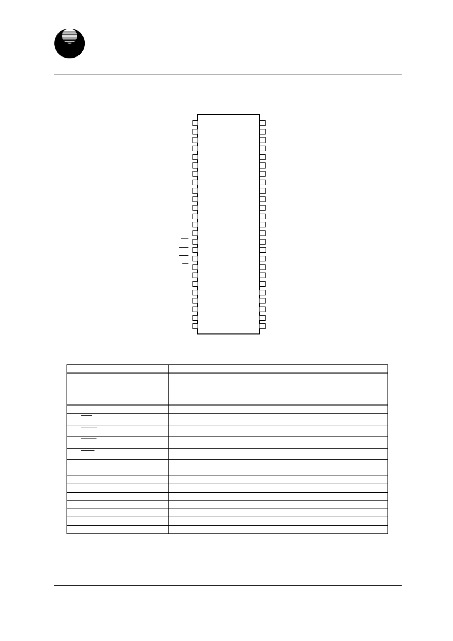
PIN ASSIGNMENT
UT52L1616
50 pin TSOP II package
V
CC
DQ0
DQ1
DQ2
DQ3
DQ4
DQ5
DQ6
DQ7
CAS
CE
WE
RAS
DQML
A10
A11
A0
A1
A2
A3
V
CC
V
SSQ
V
CCQ
V
SSQ
V
CCQ
10
11
12
13
14
15
16
17
18
19
20
25
24
23
22
21
1
2
3
4
5
6
7
8
9
40
39
38
37
36
35
34
33
32
31
30
29
28
27
26
50
49
48
47
46
45
44
43
42
41
Vss
DQ15
DQ14
DQ13
DQ12
DQMU
DQ11
DQ10
DQ9
DQ8
NC
CLK
CKE
NC
A7
A6
A5
A4
Vss
A9
A8
V
SSQ
V
CCQ
V
SSQ
V
CCQ
PIN DESCRIPTION
Pin name
Function
A0 to A11
Address input
Row address A0 to A10
Column address A0 to A7
Bank select address A11
DQ0 to DQ15
Data-input/output
CE
Chip select
CAS
Column address strobe command
RAS
Row address strobe command
WE
Write enable command
DQMU
DQML
Upper byte input/output mask
Lower byte input/output mask
CLK Clock
input
CKE Clock
enable
V
CC
Power for internal circuit
Vss
Ground for internal circuit
VccQ
Power for I/O circuit
VssQ
Ground for I/O circuit
NC No
connection
UTRON
UT52L1616
Preliminary Rev. 0.91
1M X 16 BIT SDRAM
UTRON TECHNOLOGY INC.
P90004
1F, No. 11, R&D Rd. II, Science-Based Industrial Park, Hsinchu, Taiwan, R. O. C.
TEL: 886-3-5777882 FAX: 886-3-5777919
3
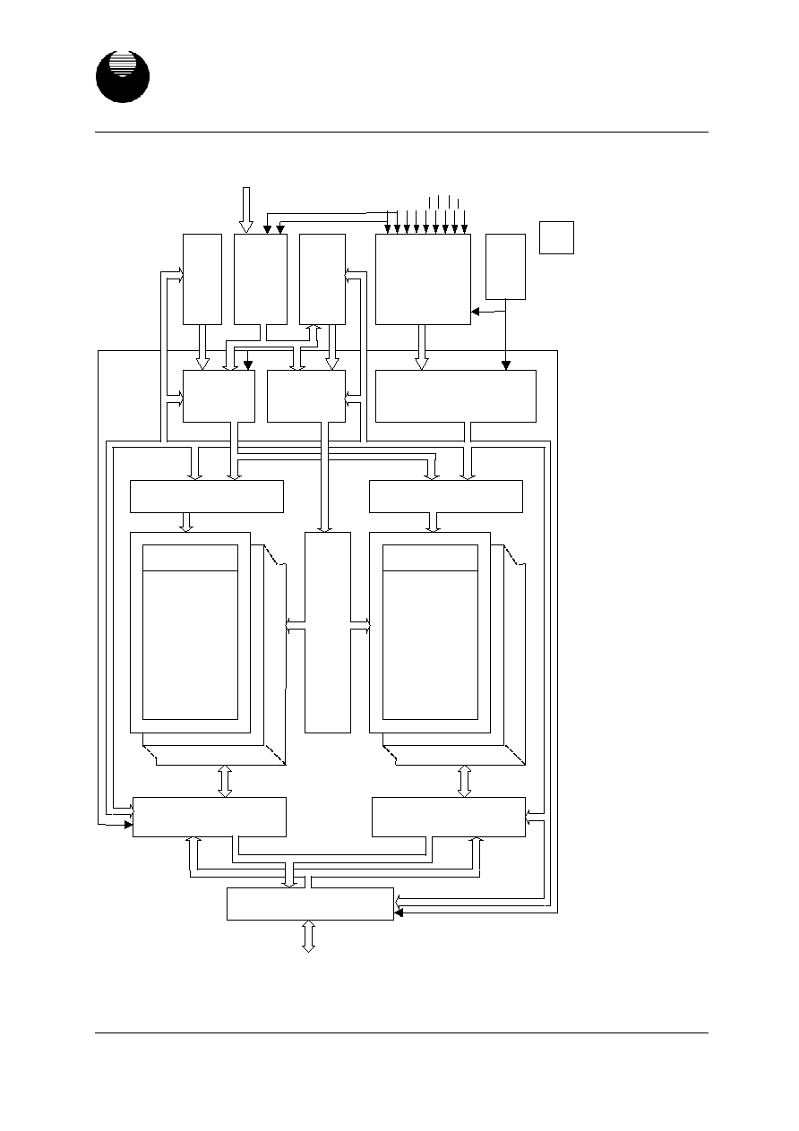
FUNCTION BLOCK DIAGRAM
Block Diagram
VCC
VSS
VPP
VBB
REG
CLK
CLOCK
BUFFER
CKE
CE
RAS
CAS
WE
DQMU
DQML
A11
A10
Bank 0 Row Control Circuit
A [0 : 9]
Cell Array
Bank 0
512K x 16 bit
Row Decoder
Column Decoder
◊
16
pairs
Cell Array
Bank 1
512K x 16 bit
Row Decoder
Sense Amp
& Write In circuit
◊
16
pairs
INPUT & OUTPUT BUFFER
Bank 1 Row Control Circuit
◊
16
DQ [0,15]
Burst
Counter
Address
Buffer
Refresh
Counter
Row
Address
Command
Buffer
Control
Circuit
Column
Address
& Pre
-
Decoder
Sense Amp
& Write In circuit

UTRON
UT52L1616
Preliminary Rev. 0.91
1M X 16 BIT SDRAM
UTRON TECHNOLOGY INC.
P90004
1F, No. 11, R&D Rd. II, Science-Based Industrial Park, Hsinchu, Taiwan, R. O. C.
TEL: 886-3-5777882 FAX: 886-3-5777919
4
PIN FUNCTIONS
CLK (input pin):
CLK is the master clock input to this pin. The other input signals are referred at CLK rising
edge.
CE
(input pin
): When
CE
is Low, the command input cycle becomes valid. When
CE
is High, all inputs are
ignored. However, internal operations (bank active, burst operations, etc.) are held.
RAS , CAS , and
WE
(input pins):
Although these pin names are the same as those of conventional
DRAMs, they function in a different way. These pins define operation commands (read, write, etc.) depending on
the combination of their voltage levels. For details, refer to the command operation section.
A0 to A10 (input pins):
Row address (AX0 to AX10) is determined by A0 to A10 level at the bank active
command cycle CLK rising edge. Column address (AY0 to AY7) is determined by A0 to A7 level at the read or
write command cycle CLK rising edge. And this column address becomes burst access start address. A10 defines
the precharge mode. When A10 = High at the precharge command cycle, both banks are precharged. But when
A10 = Low at the precharge command cycle, only the bank that is selected by A11 (BS) is precharged.
A11 (input pin):
A11 is a bank select signal (BS). The memory array of the UT52L1616 is divided into bank 0
and bank 1, both which contain 512 K x 16 bits. If A11 is Low, bank 0 is selected, and if A11 is High, bank 1 is
selected.
CKE (input pin):
This pin determines whether or not the next CLK is valid. If CKE is High, the next CLK rising
edge is valid. If CKE is Low, the next CLK rising edge is invalid. This pin is used for power down and clock
suspend modes.
DQMU/DQML (input pins):
DQMU controls upper byte and DQML controls lower byte input/output buffers.
Read operation:
If DQMU/DQML is High, the output buffer becomes High-Z. If the DQMU/DQML is Low, the
output buffer becomes Low-Z.
Write operation:
If DQMU/DQML is High, the previous data is held (the new data is not written).If
DQMU/DQML is Low, the data is written.
DQ0 to DQ15 (I/O pins):
Data is input to and output from these pins. These pins are the same as those of a
conventional DRAM.
Vcc and VccQ (power supply pins):
3.3V is applied. (Vcc is for the internal circuit and VccQ is for the
output buffer.)
Vss and VssQ (power supply pins):
Ground is connected. (Vss is for the internal circuit and VssQ is for the
output buffer.)
UTRON
UT52L1616
Preliminary Rev. 0.91
1M X 16 BIT SDRAM
UTRON TECHNOLOGY INC.
P90004
1F, No. 11, R&D Rd. II, Science-Based Industrial Park, Hsinchu, Taiwan, R. O. C.
TEL: 886-3-5777882 FAX: 886-3-5777919
5
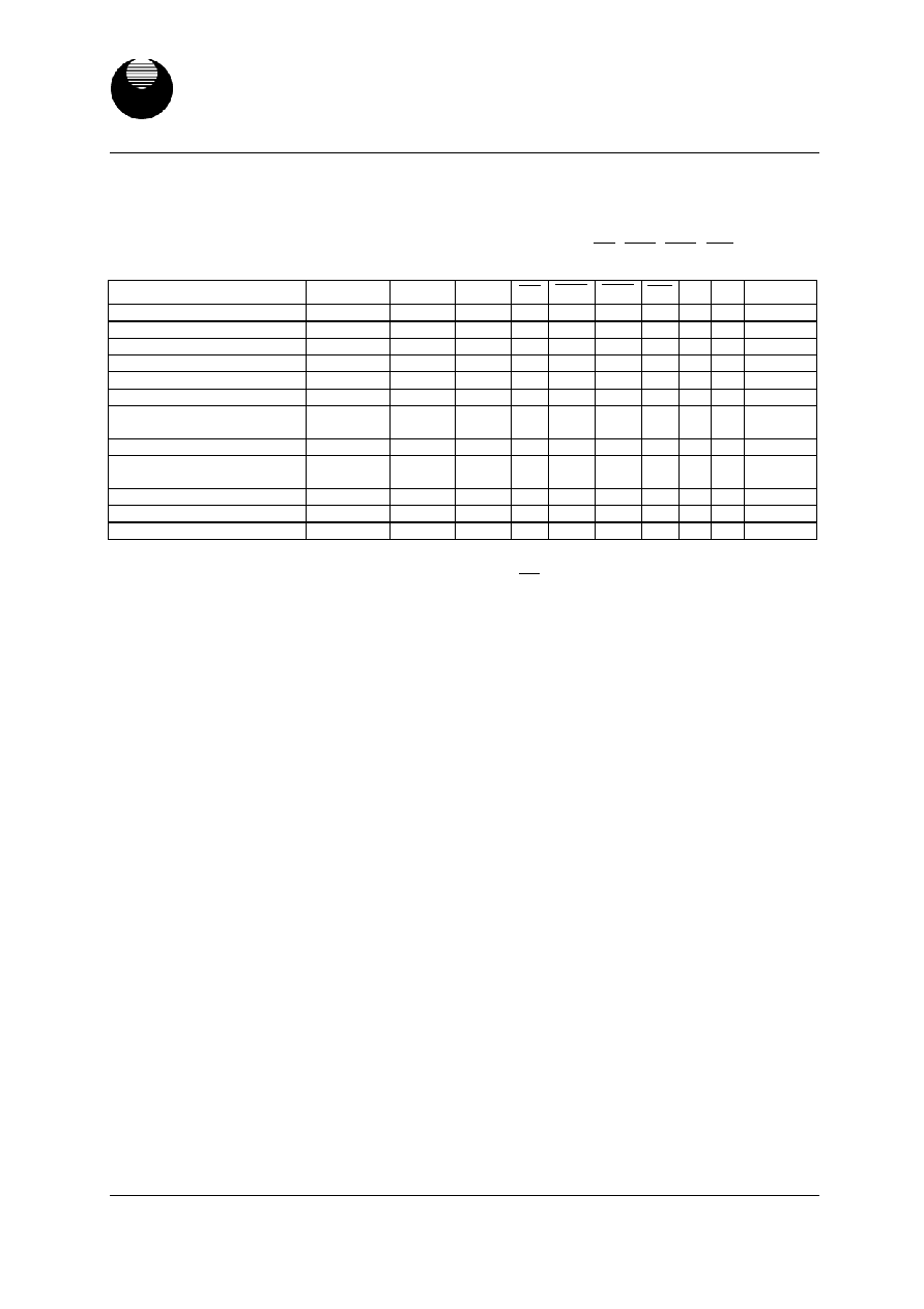
COMMAND OPERATION
Command Truth Table
The synchronous DRAM recognizes the following commands specified by the
CE
,
CAS
,
RAS
,
WE
and address pins.
Function
Symbol
CKE n-1 CKe n
CE
RAS
CAS
WE
A11 A10 A0 to A9
Ignore command
DESL
H
x
H
x
x
x
x
x
x
Mode register set
MRS
H
x
L
L
L
L
V
V
V
Refresh REF/SELF
H
V
L
L
L
H
x
x
x
Precharge select bank
PRE
H
x
L
L
H
L
V
L
x
Precharge all bank
PALL
H
x
L
L
H
L
x
H
x
Bank active
ACT
H
x
L
L
H
H
V
V
V
Column address and write
command
WRIT H x
L
H
L
L
V
L V
Write with auto-precharge
WRITA
H
x
L
H
L
L
V
H
V
Column address and read
command
READ
H
x L H L H V
L V
Read with auto-precharge
READA
H
x
L
H
L
H
V
H
V
Burst stop in full page
BST
H
x
L
H
H
L
x
x
x
No operation
NOP
H
x
L
H
H
H
x
x
x
Note: H: V
IH
. L: V
IL
. x: V
IH
or V
IL
. V: Valid address input.
Ignore Command [DESL]:
When this command is set (
CE
is High), the synchronous DRAM ignore
command input at the clock. However, the internal status is held.
Mode register set [MRS]:
Synchronous DRAM has a mode register that defines how it operates. The mode
register is specified by the address pins (A0 to A11) at the mode register set cycle. For details, refer to the mode
register configuration. After power on, the contents of the mode register are undefined, execute the mode register
set command to set up the mode register.
Refresh [REF/SELF]:
This command starts the refresh operation. There are two types of refresh operation, the
one is auto refresh, and the other is self refresh. For details, refer to the CKE truth table section.
Precharge selected bank [PRE]:
This command starts precharge operation for the bank selected by A11. If
A11 is Low, bank 0 is selected. If A11 is High, bank 1 is selected.
Precharge all banks [PALL]:
This command starts a precharge operation for all banks.
Row address strobe and bank activate [ACT]:
This command activates the bank that is selected by A11
(BS) and determines the row address (AX0 to AX10). When A11 is Low, bank 0 is activated. When A11 is High,
bank 1 is activated.
Column address strobe and write command [WRIT]:
This command starts a write operation. When the
burst write mode is selected, the column address (AY0 to AY7) and the bank select address (A11) become the
burst write start address. When the single write mode is selected, data is only written to the location specified by
the column address (AY0 to AY7) and the bank select address (A11).
Write with auto precharge [WRIT A]:
This command automatically performs a precharge operation after a
burst write with a length of 1, 2, 4 or 8.
Column address strobe and read command [READ]:
This command starts a read operation. In addition,
the start address of burst read is determined by the column address (AY0 to AY7) and the bank select address
(BS). After the read operation, the output buffer becomes High-Z.