UTRON
UT61256C
Rev. 1.4
32K X 8 BIT HIGH SPEED CMOS SRAM
UTRON TECHNOLOGY INC.
P80031
1F, No. 11, R&D Rd. II, Science-Based Industrial Park, Hsinchu, Taiwan, R. O. C.
TEL: 886-3-5777882 FAX: 886-3-5777919
1
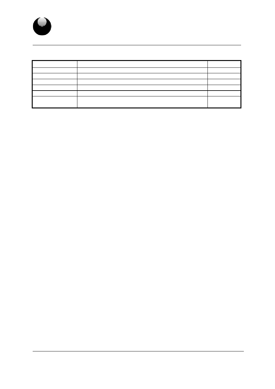
REVISION HISTORY
REVISION DESCRIPTION DATE
Preliminary Rev. 0.1
Original
May 3 ,2001
Rev. 1.0
Delete STSOP package
Jul 27,2001
Rev. 1.1
Add STSOP package
Sep 27,2001
Rev. 1.2
Revised STSOP package
Feb 1,2002
Rev. 1.3
Add under/overshoot range of V
IL
& V
IH
Nov
27,2002
Rev. 1.4
Add package 28-pin 300 mil skinny PDIP
& Package outline dimension
Jan 10,2003

UTRON
UT61256C
Rev. 1.4
32K X 8 BIT HIGH SPEED CMOS SRAM
UTRON TECHNOLOGY INC. P80031
1F, No. 11, R&D Rd. II, Science-Based Industrial Park, Hsinchu, Taiwan, R. O. C.
TEL: 886-3-5777882 FAX: 886-3-5777919
2
FEATURES
Fast access time : 8/10/12/15 ns (max.)
Low power operating : 80 mA (typical)
Single 5V power supply
All inputs and outputs TTL compatible
Fully static operation
Three state outputs
Package : 28-pin 300 mil SOJ
28-pin 8mm�13.4mm STSOP
28-pin 300 mil skinny PDIP
GENERAL DESCRIPTION
The UT61256C is a 262,144-bit high-speed
CMOS static random access memory organized
as 32,768 words by 8 bits. It is fabricated using
high performance, high reliability CMOS
technology.
The UT61256C is designed for high-speed
system applications. It is particularly suited for
use in high-density high-speed system
applications.
The UT61256C operates from a single 5V power
supply and all inputs and outputs are fully TTL
compatible.
FUNCTIONAL BLOCK DIAGRAM
DECODER
I/O DATA
CIRCUIT
CONTROL
CIRCUIT
32K
�
8
MEMORY
ARRAY
COLUMN I/O
A0-A14
Vcc
Vss
I/O1-I/O8
CE
OE
WE
UTRON
UT61256C
Rev. 1.4
32K X 8 BIT HIGH SPEED CMOS SRAM
UTRON TECHNOLOGY INC. P80031
1F, No. 11, R&D Rd. II, Science-Based Industrial Park, Hsinchu, Taiwan, R. O. C.
TEL: 886-3-5777882 FAX: 886-3-5777919
3
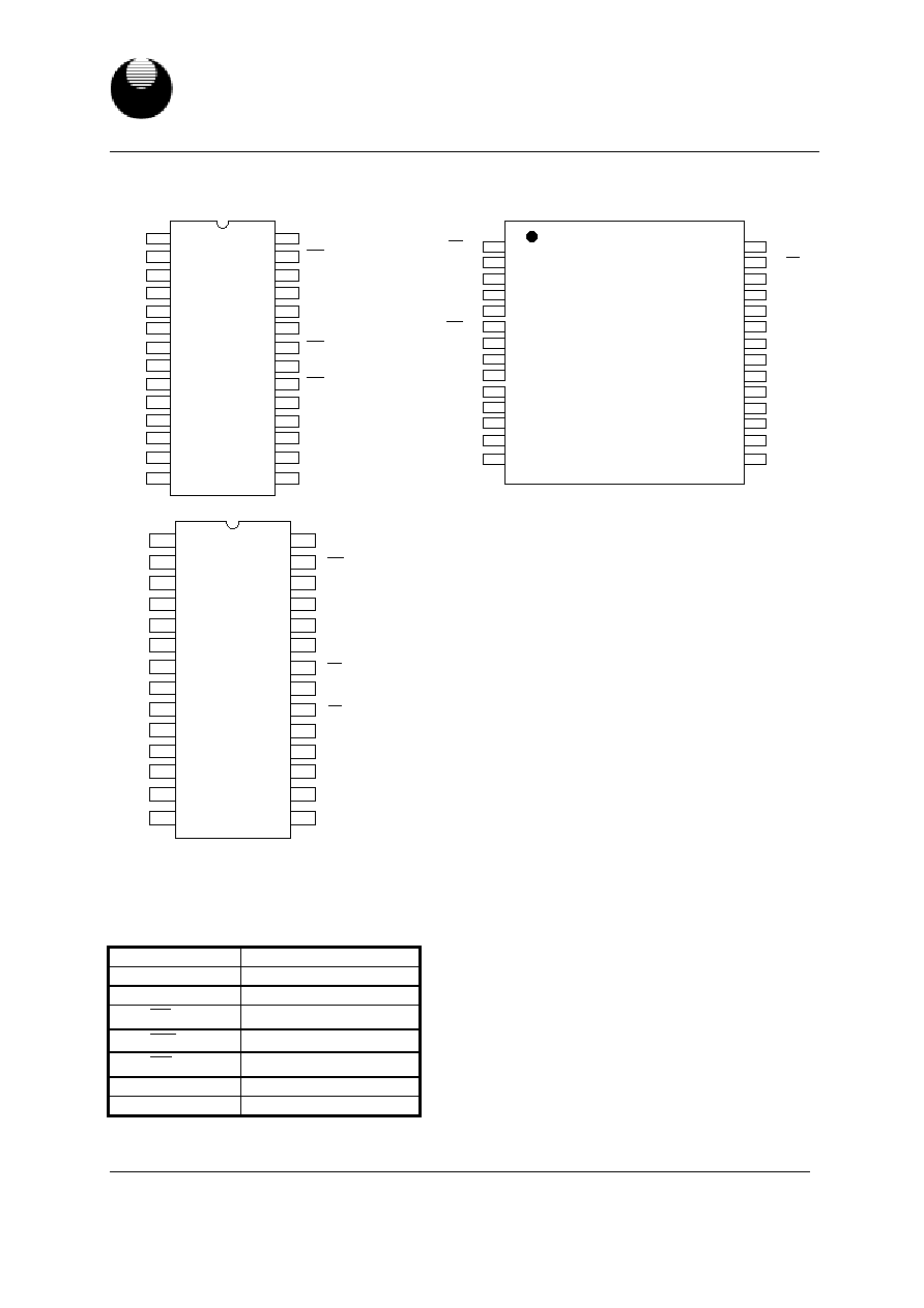
PIN CONFIGURATION
A12
A7
A6
A5
A4
A3
A2
A1
A0
I/O1
I/O2
Vcc
A8
A9
A11
A10
I/O8
I/O7
I/O6
I/O5
I/O4
I/O3
Vss
UT61256C
SOJ
28
14
13
12
11
10
9
8
7
6
5
4
3
2
1
17
16
15
20
19
18
22
23
24
25
26
27
21
A13
A14
WE
OE
CE
I/O4
A11
A9
A8
A13
I/O3
A10
A14
A12
A7
A6
A5
Vcc
I/O8
I/O7
I/O6
I/O5
Vss
I/O2
I/O1
A0
A1
A2
A4
A3
UT61256C
STSOP
28
14
13
12
11
10
9
8
7
6
5
4
3
2
1
17
16
15
20
19
18
22
23
24
25
26
27
21
OE
WE
CE
A12
A7
A6
A5
A4
A3
A2
A1
A0
I/O1
I/O2
Vcc
A8
A9
A11
A10
I/O8
I/O7
I/O6
I/O5
I/O4
I/O3
Vss
UT61256C
skinny PDIP
28
14
13
12
11
10
9
8
7
6
5
4
3
2
1
17
16
15
20
19
18
22
23
24
25
26
27
21
CE
WE
OE
A13
A14
PIN DESCRIPTION
SYMBOL DESCRIPTION
A0 - A14
Address Inputs
I/O1 - I/O8
Data Inputs/Outputs
CE
Chip Enable Input
WE
Write Enable Input
OE
Output Enable Input
V
CC
Power
Supply
V
SS
Ground
UTRON
UT61256C
Rev. 1.4
32K X 8 BIT HIGH SPEED CMOS SRAM
UTRON TECHNOLOGY INC.
P80031
1F, No. 11, R&D Rd. II, Science-Based Industrial Park, Hsinchu, Taiwan, R. O. C.
TEL: 886-3-5777882 FAX: 886-3-5777919
4
ABSOLUTE MAXIMUM RATINGS*
PARAMETER
SYMBOL
RATING
UNIT
Terminal Voltage with Respect to Vss
V
TERM
-0.5 to +6.5
V
Operating Temperature
T
A
0 to +70
Storage Temperature
T
STG
-65 to +150
Power Dissipation
P
D
1
W
DC Output Current
I
OUT
50
mA
Soldering Temperature (under 10 sec)
Tsolder
260
*Stress greater than those listed under "Absolute Maximum Ratings" may cause permanent damage to the device. This is a
stress rating only and functional operation of the device or any other conditions above those indicated in the operational
sections of this specification is not implied. Exposure to the absolute maximum rating conditions for extended period may
affect device reliability.
TRUTH TABLE
MODE
CE
OE
WE
I/O OPERATION
SUPPLY CURRENT
Standby
H
X
X
High - Z
I
SB
,
I
SB1
Output Disable
L
H
H
High - Z
I
CC
Read L
L
H
D
OUT
I
CC
Write L
X
L
D
IN
I
CC
Note: H = V
IH
, L=V
IL
, X = Don't care.
DC ELECTRICAL CHARACTERISTICS
(V
CC
= 5V
�
10%, T
A
= 0
to 70
)
PARAMETER
SYMBOL TEST CONDITION
MIN.
MAX.
UNIT
Input High Voltage
V
IH
2.2
V
CC
+0.5 V
Input Low Voltage
V
IL
-
0.5
0.8
V
Input Leakage Current
I
LI
V
SS
V
IN
V
CC
- 1
1
�A
Output Leakage Current
I
LO
V
SS
V
I/O
V
CC
CE =V
IH
or OE =V
IH
or
WE
=V
IL
- 1
1
�A
Output High Voltage
V
OH
I
OH
= - 4mA
2.4
-
V
Output Low Voltage
V
OL
I
OL
= 8mA
-
0.4
V
- 8
-
190
mA
- 10
-
180
mA
- 12
-
160
mA
Operating Power
Supply Current
I
CC
Cycle time=Min.
CE
= V
IL ,
I
I/O
=
0mA
- 15
-
140
mA
Standby Current (TTL)
I
SB
CE
= V
IH
-
30
mA
Standby Current (CMOS)
I
SB1
CE
V
CC
-0.2V
-
5
mA
Notes:
1. Overshoot : Vcc+2.0v for pulse width less than 6ns.
2. Undershoot : Vss-2.0v for pulse width less than 6ns.
3. Overshoot and Undershoot are sampled, not 100% tested.

UTRON
UT61256C
Rev. 1.4
32K X 8 BIT HIGH SPEED CMOS SRAM
UTRON TECHNOLOGY INC. P80031
1F, No. 11, R&D Rd. II, Science-Based Industrial Park, Hsinchu, Taiwan, R. O. C.
TEL: 886-3-5777882 FAX: 886-3-5777919
5
CAPACITANCE
(TA=25
, f=1.0MHz)
PARAMETER
SYMBOL MIN.
MAX.
UNIT
Input Capacitance
C
IN
-
8
pF
Input/Output Capacitance
C
I/O
-
10
pF
Note : These parameters are guaranteed by device characterization, but not production tested.
AC TEST CONDITIONS
Input Pulse Levels
0V to 3.0V
Input Rise and Fall Times
3ns
Input and Output Timing Reference Levels
1.5V
Output Load
C
L
=30pF, I
OH
/I
OL
=-4mA/8mA
AC ELECTRICAL CHARACTERISTICS
(V
CC
= 5V
�
10% , T
A
= 0
to 70
)
(1) READ CYCLE
UT61256C
-8
UT61256C
-10
UT61256C
-12
UT61256C
-15
PARAMETER
SYMBOL
MIN. MAX. MIN. MAX. MIN. MAX. MIN. MAX.
UNIT
Read Cycle Time
t
RC
8 - 10 - 12 - 15 - ns
Address Access Time
t
AA
- 8 - 10 - 12 - 15 ns
Chip Enable Access Time
t
ACE
- 8 - 10 - 12 - 15 ns
Output Enable Access Time
t
OE
- 4 - 5 - 6 - 7 ns
Chip Enable to Output in Low Z
t
CLZ*
2 - 2 - 3 - 4 - ns
Output Enable to Output in Low Z
t
OLZ*
0 - 0 - 0 - 0 - ns
Chip Disable to Output in High Z
t
CHZ*
- 4 - 5 - 6 - 7 ns
Output Disable to Output in High Z
t
OHZ*
- 4 - 5 - 6 - 7 ns
Output Hold from Address Change
t
OH
3 - 3 - 3 - 3 - ns
(2) WRITE CYCLE
UT61256C
-8
UT61256C
-10
UT61256C
-12
UT61256C
-15
PARAMETER
SYMBOL
MIN. MAX. MIN. MAX. MIN. MAX. MIN. MAX.
UNIT
Write Cycle Time
t
WC
8 - 10 - 12 - 15 - ns
Address Valid to End of Write
t
AW
6.5 - 8 - 10 - 12 - ns
Chip Enable to End of Write
t
CW
6.5 - 8 - 10 - 12 - ns
Address Set-up Time
t
AS
0 - 0 - 0 - 0 - ns
Write Pulse Width
t
WP
6.5 - 8 - 9 - 10 - ns
Write Recovery Time
t
WR
0 - 0 - 0 - 0 - ns
Data to Write Time Overlap
t
DW
5 - 6 - 7 - 8 - ns
Data Hold from End of Write Time
t
DH
0 - 0 - 0 - 0 - ns
Output Active from End of Write
t
OW*
1.5 - 2 - 3 - 4 - ns
Write to Output in High Z
t
WHZ*
5 - 6 - 7 - 8 ns
*These parameters are guaranteed by device characterization, but not production tested.

UTRON
UT61256C
Rev. 1.4
32K X 8 BIT HIGH SPEED CMOS SRAM
UTRON TECHNOLOGY INC. P80031
1F, No. 11, R&D Rd. II, Science-Based Industrial Park, Hsinchu, Taiwan, R. O. C.
TEL: 886-3-5777882 FAX: 886-3-5777919
6
TIMING WAVEFORMS
READ CYCLE 1
(Address Controlled)
(1,2,4)
t
RC
Address
DOUT
Data Valid
t
AA
t
OH
t
OH
READ CYCLE 2
(
CE
and
OE
Controlled)
(1,3,5,6)
t
RC
t
AA
t
ACE
t
OE
t
CHZ
t
OHZ
t
CLZ
t
OH
t
OLZ
HIGH-Z
Data Valid
HIGH-Z
Address
CE
OE
Dout
Notes :
1. WE is HIGH for read cycle.
2. Device is continuously selected
CE
=V
IL.
3. Address must be valid prior to or coincident with
CE
transition; otherwise t
AA
is the limiting parameter.
4.
OE
is LOW.
5. t
CLZ
, t
OLZ
, t
CHZ
and t
OHZ
are specified with C
L
= 5pF. Transition is measured
�
500mV from steady state.
6. At any given temperature and voltage condition, t
CHZ
is less than t
CLZ
, t
OHZ
is less than t
OLZ.

UTRON
UT61256C
Rev. 1.4
32K X 8 BIT HIGH SPEED CMOS SRAM
UTRON TECHNOLOGY INC. P80031
1F, No. 11, R&D Rd. II, Science-Based Industrial Park, Hsinchu, Taiwan, R. O. C.
TEL: 886-3-5777882 FAX: 886-3-5777919
7
WRITE CYCLE 1 (
WE
Controlled) (1,2,3,5,6)
t
WC
t
AW
t
CW
t
AS
t
WP
t
WHZ
t
OW
t
DW
t
DH
t
WR
Address
CE
WE
Dout
Din
Data Valid
High-Z
(4)
(4)
WRITE CYCLE 2
(
CE
Controlled)
(1,2,5)
t
WC
t
AW
t
CW
t
AS
t
WR
t
WP
t
WHZ
t
DW
t
DH
Data Valid
Address
CE
WE
Dout
Din
High-Z
Notes :
1. WE and
CE
must be HIGH during all address transitions.
2. A write occurs during the overlap of a low
CE
and a low WE .
3. During a WE controlled with write cycle with
OE
LOW, t
WP
must be greater than t
WHZ
+t
DW
to allow the drivers to turn off
and data to be placed on the bus.
4. During this period, I/O pins are in the output state, and input singals must not be applied.
5. If the
CE
low transition occurs simultaneously with or after WE low transition, the outputs remain in a high impedance state.
6. t
OW
and t
WHZ
are specified with C
L
= 5pF. Transition is measured
�
500mV from steady state.

UTRON
UT61256C
Rev. 1.4
32K X 8 BIT HIGH SPEED CMOS SRAM
UTRON TECHNOLOGY INC. P80031
1F, No. 11, R&D Rd. II, Science-Based Industrial Park, Hsinchu, Taiwan, R. O. C.
TEL: 886-3-5777882 FAX: 886-3-5777919
8
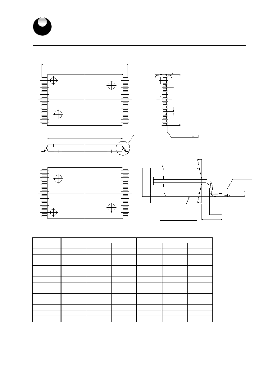
PACKAGE OUTLINE DIMENSION
28 pin 300 mil SOJ Package Outline Dimension
1
28
14
15
A2
L
C
XX
X
Note:
1. S/E/D DIM NOT INCLUDEING MOLD FLASH.
2.
THE END FLASH IN PACKAGE LENGTHWISE IS
NOT MORE THAN 10 MILS EACH SIDE
UNIT
SYMBOL
INCH(REF) MM(BASE)
A
0.140 (MAX)
3.556 (MAX)
A1
0.026 (MIN)
0.660 (MIN)
A2
0.100
�
0.005 2.540
�
0.127
B
0.018
�
0.003 0.457
�
0.076
B1
0.028
�
0.003 0.711
�
0.076
c
0.010
�
0.003 0.254
�
0.076
D
0.710
�
0.010 18.03
�
0.254
E
0.337
�
0.010 8.560
�
0.254
E1
0.300
�
0.005 7.620
�
0.127
e
0.050
�
0.003 1.270
�
0.076
L
0.087
�
0.010 2.210
�
0.254
S
0.030
�
0.004 0.762
�
0.102
Y
0.003 (MAX)
0.076 (MAX)
UTRON
UT61256C
Rev. 1.4
32K X 8 BIT HIGH SPEED CMOS SRAM
UTRON TECHNOLOGY INC. P80031
1F, No. 11, R&D Rd. II, Science-Based Industrial Park, Hsinchu, Taiwan, R. O. C.
TEL: 886-3-5777882 FAX: 886-3-5777919
9
28 pin 8x13.4mm STSOP Package Outline Dimension
1
14
15
28
cL
HD
D
"A"
b
E
e
12
�
(2x)
12
�
(2x)
Seating Plane
y
28
15
14
1
c
A2
A1
L
A
0.
25
4
0
GAUGE PLANE
12
�
(2X)
12
�
(2X)
SEATING PLANE
"A" DATAIL VIEW
L1
DIMENSIONS IN MILLIMETERS
DIMENSIONS IN INCHES
SYMBOLS
MIN NOM MAX MIN NOM MAX
A 1.00 1.10 1.20 0.040 0.043 0.047
A1 0.05 - 0.15
0.002 - 0.006
A2 0.91 1.00 1.05 0.036 0.039 0.041
b 0.17 0.22 0.27 0.007 0.009 0.011
c 0.10 0.15 0.20 0.004 0.006 0.008
HD 13.20 13.40 13.60 0.520 0.528 0.535
D
11.70 11.80 11.90 0.461 0.465 0.469
E 7.90 8.00 8.10 0.311 0.315 0.319
e -
0.55
- -
0.0216
-
L 0.30 0.50 0.70 0.012 0.020 0.028
L1 0.675 - - 0.027 - -
Y 0.00 - 0.076
0.000 - 0.003
0
o
3
o
5
o
0
o
3
o
5
o
UTRON
UT61256C
Rev. 1.4
32K X 8 BIT HIGH SPEED CMOS SRAM
UTRON TECHNOLOGY INC. P80031
1F, No. 11, R&D Rd. II, Science-Based Industrial Park, Hsinchu, Taiwan, R. O. C.
TEL: 886-3-5777882 FAX: 886-3-5777919
10
PACKAGE OUTLINE DIMENSION
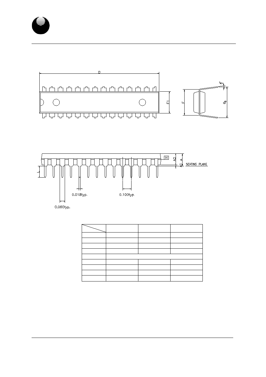
28 pin 300 mil skinny PDIP Package Outline Dimension
UNIT
SYMBOL
MIN NOR. MAX
A - - 0.210
A1 0.015
-
-
A2 0.125 0.130 0.135
D 1.385 1.390 1.400
E 0.310
BSC
E1 0.283 0.288 0.293
L 0.115 0.130 0.150
eB 0.330 0.350 0.370
�
0
7
15
Note
1. JEDEC OUTLINE
N / A

UTRON
UT61256C
Rev. 1.4
32K X 8 BIT HIGH SPEED CMOS SRAM
UTRON TECHNOLOGY INC. P80031
1F, No. 11, R&D Rd. II, Science-Based Industrial Park, Hsinchu, Taiwan, R. O. C.
TEL: 886-3-5777882 FAX: 886-3-5777919
11
ORDERING INFORMATION
PART NO.
ACCESS TIME (ns)
PACKAGE
UT61256CJC-8
8
28 PIN SOJ
UT61256CJC-10
10
28 PIN SOJ
UT61256CJC-12
12
28 PIN SOJ
UT61256CJC-15
15
28 PIN SOJ
UT61256CLS-8
8
28 PIN STSOP
UT61256CLS-10
10
28 PIN STSOP
UT61256CLS-12
12
28 PIN STSOP
UT61256CLS-15
15
28 PIN STSOP
UT61256CKC-8
8
28 PIN SKINNY PDIP
UT61256CKC-10
10
28 PIN SKINNY PDIP
UT61256CKC-12
12
28 PIN SKINNY PDIP
UT61256CKC-15
15
28 PIN SKINNY PDIP

UTRON
UT61256C
Rev. 1.4
32K X 8 BIT HIGH SPEED CMOS SRAM
UTRON TECHNOLOGY INC. P80031
1F, No. 11, R&D Rd. II, Science-Based Industrial Park, Hsinchu, Taiwan, R. O. C.
TEL: 886-3-5777882 FAX: 886-3-5777919
12
THIS PAGE IS LEFT BLANK INTENTIONALLY.