UTRON
UT61L6416
Rev. 1.1
64K X 16 BIT HIGH SPEED CMOS SRAM
UTRON TECHNOLOGY INC. P80072
1F, No. 11, R&D Rd. II, Science-Based Industrial Park, Hsinchu, Taiwan, R. O. C.
TEL: 886-3-5777882 FAX: 886-3-5777919
1
REVISION HISTORY
REVISION DESCRIPTION Date
Preliminary Rev. 0.4 Original.
Mar, 2001
Preliminary Rev. 0.5 1.The symbols CE# and OE# and WE# are revised as. CE and
OE and
WE
.
2.Separate Industrial and Commercial SPEC.
3.Add access time 15ns range.
4.Delete SOJ package.
Aug 31,2001
Rev. 1.0
1.Revised CMOS low power operating :
Operating current : 195 150mA (max.)
Standby current : 30mA (max.) 1mA (Typ.)
2.Revised power supply : 3.0~3.6V 3.15~3.6V
3.Revised DC CHARACTERISTICE
I
CC
≠8ns (max) : 200 150mA
I
CC
≠10ns (max) : 195 120mA
I
CC
≠12ns (max) : 190 100mA
I
CC
≠15ns (max) : 150 80 mA
I
SB
(max) : 30 10mA, I
SB
(typ) : NA 3mA
I
SB1
(max) : 10 3mA, I
SB1
(typ) : NA 1mA
I
SB1
(max)<1 mA for special order
4. Add order information for lead free product
May 20,2003
Rev. 1.1
1.Add Extended temperature : -20
~80
Jul 03,2003
UTRON
UT61L6416
Rev. 1.1
64K X 16 BIT HIGH SPEED CMOS SRAM
UTRON TECHNOLOGY INC. P80072
1F, No. 11, R&D Rd. II, Science-Based Industrial Park, Hsinchu, Taiwan, R. O. C.
TEL: 886-3-5777882 FAX: 886-3-5777919
2
FEATURES
Fast access time :
8ns for Vcc=3.15V~3.6V
10/12/15ns for Vcc=3.0V~3.6V
CMOS low power operating :
Operating current : 150mA (max.)
Standby current : 1mA (typ.)
Single 3.15~3.6V power supply
Operating temperature :
Commercial : 0
~70
Extended : -20
~80
All TTL compatible inputs and outputs
Fully static operation
Three state outputs
Data byte control :
LB
(I/O0~I/O7)
UB (I/O8~I/O15)
Package : 44-pin 400mil TSOP
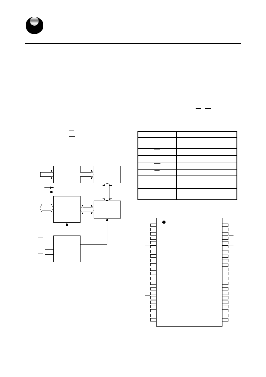
FUNCTIONAL BLOCK DIAGRAM
DECODER
I/O DATA
CIRCUIT
CONTROL
CIRCUIT
64K
◊
16 bit
MEMORY
ARRAY
COLUMN I/O
A0-A15
Vcc
Vss
I/O0-I/O15
CE
OE
UB
LB
WE
GENERAL DESCRIPTION
The UT61L6416 is a 1,048,576-bit high speed CMOS
static random access memory organized as 65,536
words by 16 bits.
The UT61L6416 operates from a single 3.15 ~ 3.6V
power supply and all inputs and outputs are fully TTL
compatible.
The UT61L6416 is designed for lower and upper byte
access by data byte control.(
LB
UB )
PIN DESCRIPTION
SYMBOL DESCRIPTION
A0 - A15
Address Inputs
I/O0 - I/O15
Data Inputs/Outputs
CE
Chip Enable Input
WE
Write Enable Input
OE
Output Enable Input
LB
Lower Byte Control
UB
Upper Byte Control
V
CC
Power
Supply
V
SS
Ground
NC No
Connection
PIN CONFIGURATION
TSOP II
A1
A2
A3
A4
I/O15
I/O0
I/O1
I/O2
Vcc
Vss
NC
NC
I/O14
I/O12
I/O13
I/O11
Vss
Vcc
I/O10
I/O9
I/O3
I/O4
28
14
13
12
11
10
9
8
7
6
5
4
3
2
1
17
16
15
20
19
18
22
23
24
25
26
27
21
A15
A0
I/O6
I/O7
A5
A6
A7
A8
A9
I/O5
I/O8
A14
A13
A12
A10
NC
34
29
30
31
32
33
44
39
40
41
42
43
35
36
37
38
A11
OE
UB
LB
WE
CE
UTRON
UT61L6416
Rev. 1.1
64K X 16 BIT HIGH SPEED CMOS SRAM
UTRON TECHNOLOGY INC. P80072
1F, No. 11, R&D Rd. II, Science-Based Industrial Park, Hsinchu, Taiwan, R. O. C.
TEL: 886-3-5777882 FAX: 886-3-5777919
3
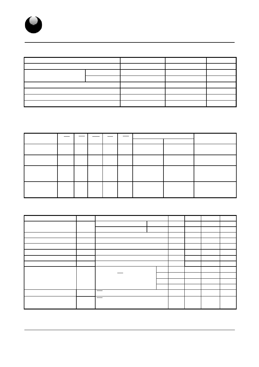
ABSOLUTE MAXIMUM RATINGS*
PARAMETER SYMBOL
RATING
UNIT
Terminal Voltage with Respect to V
SS
V
TERM
-0.5 to 4.6
V
Commercial
T
A
0 to 70
Operating Temperature
Extended
T
A
-20 to 80
Storage Temperature
T
STG
-65 to 150
Power Dissipation
P
D
1
W
DC Output Current
I
OUT
50
mA
Soldering Temperature (under 10 secs)
Tsolder
260
*Stresses greater than those listed under "Absolute Maximum Ratings" may cause permanent damage to the device. This is a stress
rating only and functional operation of the device or any other conditions above those indicated in the operational sections of this
specification is not implied. Exposure to the absolute maximum rating conditions for extended period may affect device reliability.
TRUTH TABLE
I/O OPERATION
MODE
CE
OE
WE
LB
UB
I/O0-I/O7 I/O8-I/O15
SUPPLY CURRENT
Standby
H
X
X
X
X
X
X
H
X
H
High ≠ Z
High ≠ Z
I
SB
, I
SB1
Output Disable
L
L
H
H
H
H
L
X
X
L
High ≠ Z
High ≠ Z
High ≠ Z
High ≠ Z
I
CC
Read
L
L
L
L
L
L
H
H
H
L
H
L
H
L
L
D
OUT
High ≠ Z
D
OUT
High ≠ Z
D
OUT
D
OUT
I
CC
Write
L
L
L
X
X
X
L
L
L
L
H
L
H
L
L
D
IN
High ≠ Z
D
IN
High ≠ Z
D
IN
D
IN
I
CC
Note: H = V
IH
, L=V
IL
, X = Don't care.
DC ELECTRICAL CHARACTERISTICS
(T
A
= 0
to 70
/ -20
to 80
(E))
PARAMETER
SYMBOL
TEST CONDITION
MIN.
TYP.
MAX.
UNIT
8
3.15
3.3
3.6
V
Power Voltage
V
CC
10/12/15
3.0
3.3
3.6
V
Input High Voltage
V
IH
2.0 - V
CC
+0.3 V
Input Low Voltage
V
IL
-0.3 - 0.8 V
Input Leakage Current
I
LI
V
SS
V
IN
V
CC
- 2
-
2
µA
Output Leakage Current
I
LO
V
SS
V
I/O
V
CC;
Output Disable
- 2
-
2
µA
Output High Voltage
V
OH
I
OH
= -4mA
2.4
-
-
V
Output Low Voltage
V
OL
I
OL
= 8mA
-
-
0.4
V
8
- - 150
mA
10
- - 120
mA
12 - - 100 mA
Operating Power
Supply Current
I
CC
Cycle time=min, 100%duty
I/O=0mA, CE =V
IL
15 - - 80 mA
Standby Current (TTL)
I
SB
CE =V
IH,
other pins =V
IL
or V
IH
- 3 10
mA
Standby Current (CMOS) I
SB1
CE =V
CC
-0.2V, other pins at 0.2V
or Vcc-0.2V
- 1 3*
4
mA
Notes:
1. Overshoot : Vcc+3.0v for pulse width less than 6ns.
2. Undershoot : Vss-3.0v for pulse width less than 6ns.
3. Overshoot and Undershoot are sampled, not 100% tested.
4. I
SB1
< 1mA for special order or requirement.
UTRON
UT61L6416
Rev. 1.1
64K X 16 BIT HIGH SPEED CMOS SRAM
UTRON TECHNOLOGY INC. P80072
1F, No. 11, R&D Rd. II, Science-Based Industrial Park, Hsinchu, Taiwan, R. O. C.
TEL: 886-3-5777882 FAX: 886-3-5777919
4
CAPACITANCE
(T
A
=25
, f=1.0MHz)
PARAMETER
SYMBOL
MIN.
MAX
UNIT
Input Capacitance
C
IN
-
6 pF
Input/Output Capacitance
C
I/O
-
8 pF
Note : These parameters are guaranteed by device characterization, but not production tested.
AC TEST CONDITIONS
Input Pulse Levels
0V to 3.0V
Input Rise and Fall Times
3ns
Input and Output Timing Reference Levels
1.5V
Output Load
C
L
= 30pF, I
OH
/I
OL
= -4mA / 8mA
AC ELECTRICAL CHARACTERISTICS
(TA =0
to 70
/ -20
to 80
(E))
(1) READ CYCLE
UT61L6416
-8
V
CC
=3.15
3.6
UT61L6416
-10
V
CC
=3.0
3.6
UT61L6416
-12
V
CC
=3.0
3.6
UT61L6416
-15
V
CC
=3.0
3.6
PARAMETER SYMBOL
MIN. MAX. MIN. MAX. MIN. MAX. MIN. MAX.
UNIT
Read Cycle Time
t
RC
8 - 10 - 12 - 15 - ns
Address Access Time
t
AA
- 8 - 10 - 12 - 15 ns
Chip Enable Access Time
t
ACE
- 8 - 10 - 12 - 15 ns
Output Enable Access Time
t
OE
- 4 - 5 - 6 - 7 ns
Chip Enable to Output in Low Z
t
CLZ*
3 - 3 - 3 - 3 - ns
Output Enable to Output in Low Z
t
OLZ*
0 - 0 - 0 - 0 - ns
Chip Disable to Output in High Z
t
CHZ*
- 4 - 5 - 6 - 7 ns
Output Disable to Output in High Z
t
OHZ*
- 4 - 5 - 6 - 7 ns
Output Hold from Address Change
t
OH
3 - 3 - 3 - 3 - ns
LB
,
UB
Access Time
t
BA
- 4 - 5 - 6 - 7 ns
LB
,
UB
to High Z Output
t
BHZ
- 4 - 5 - 6 - 7 ns
LB
,
UB
to Low Z Output
t
BLZ
0 - 0 - 0 - 0 - ns
(2) WRITE CYCLE
UT61L6416
-8
V
CC
=3.15
3.6
UT61L6416
-10
V
CC
=3.0
3.6
UT61L6416
-12
V
CC
=3.0
3.6
UT61L6416
-15
V
CC
=3.0
3.6
PARAMETER SYMBOL
MIN. MAX. MIN. MAX. MIN. MAX. MIN. MAX.
UNIT
Write Cycle Time
t
WC
8 - 10 - 12 - 15 - ns
Address Valid to End of Write
t
AW
7 - 8 - 9 - 10 - ns
Chip Enable to End of Write
t
CW
7 - 8 - 9 - 10 - ns
Address Set-up Time
t
AS
0 - 0 - 0 - 0 - ns
Write Pulse Width
t
WP
7 - 8 - 9 - 10 - ns
Write Recovery Time
t
WR
0 - 0 - 0 - 0 - ns
Data to Write Time Overlap
t
DW
5.5 - 6 - 7 - 8 - ns
Data Hold from End of Write Time
t
DH
0 - 0 - 0 - 0 - ns
Output Active from End of Write
t
OW*
3 - 3 - 3 - 3 - ns
Write to Output in High Z
t
WHZ*
- 4 - 5 - 6 - 7 ns
LB
,
UB
Valid to End of Write
t
BW
7 - 8 - 9 - 10 - ns
*These parameters are guaranteed by device characterization, but not production tested.
UTRON
UT61L6416
Rev. 1.1
64K X 16 BIT HIGH SPEED CMOS SRAM
UTRON TECHNOLOGY INC. P80072
1F, No. 11, R&D Rd. II, Science-Based Industrial Park, Hsinchu, Taiwan, R. O. C.
TEL: 886-3-5777882 FAX: 886-3-5777919
5
TIMING WAVEFORMS
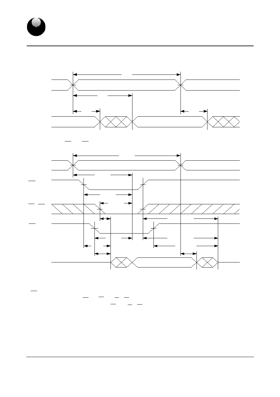
READ CYCLE 1
(Address Controlled)
(1,2)
t
RC
t
AA
Data Valid
Address
Dout
t
OH
t
OH
Previous data valid
READ CYCLE 2
(
CE
and
OE
Controlled)
(1,3,4,5)
t
RC
t
AA
t
ACE
t
BLZ
t
OE
t
OHZ
t
CLZ
t
BHZ
t
OH
t
OLZ
High-Z
Data Valid
High-Z
t
BA
t
CHZ
Address
Dout
CE
LB , UB
OE
Notes :
1.
WE
is high for read cycle.
2.Device is continuously selected OE =low, CE =low,
LB
or UB =low
.
3.Address must be valid prior to or coincident with CE =low
,
LB
or UB =low transition; otherwise t
AA
is the limiting parameter.
4.t
CLZ
, t
BLZ
, t
OLZ
, t
CHZ
, t
BHZ
and t
OHZ
are specified with C
L
=5pF. Transition is measured
±
500mV from steady state.
5.At any given temperature and voltage condition, t
CHZ
is less than t
CLZ
, t
BHZ
is less than t
BLZ
, t
OHZ
is less than t
OLZ
.