Vishay General Semiconductor
SMBG5.0 thru SMG188CA
Document Number 88456
05-Jul-06
www.vishay.com
1
Surface Mount T
RANS
Z
ORB
Æ
Transient Voltage Suppressors
FEATURES
∑ Low profile package
∑ Ideal for automated placement
∑ Glass passivated chip junction
∑ Available in Unidirectional and Bidirectional
∑ 600 W peak pulse power capability with a
10/1000 µs waveform, repetitive rate (duty cycle):
0.01 %
∑ Excellent clamping capability
∑ Very fast response time
∑ Low incremental surge resistance
∑ Meets MSL level 1, per J-STD-020C, LF max peak
of 260 ∞C
∑ Solder Dip 260 ∞C, 40 seconds
∑ Component in accordance to RoHS 2002/95/EC
and WEEE 2002/96/EC
TYPICAL APPLICATIONS
Use in sensitive electronics protection against voltage
transients induced by inductive load switching and
lighting on ICs, MOSFET, signal lines of sensor units
for consumer, computer, industrial, automotive and
telecommunication.
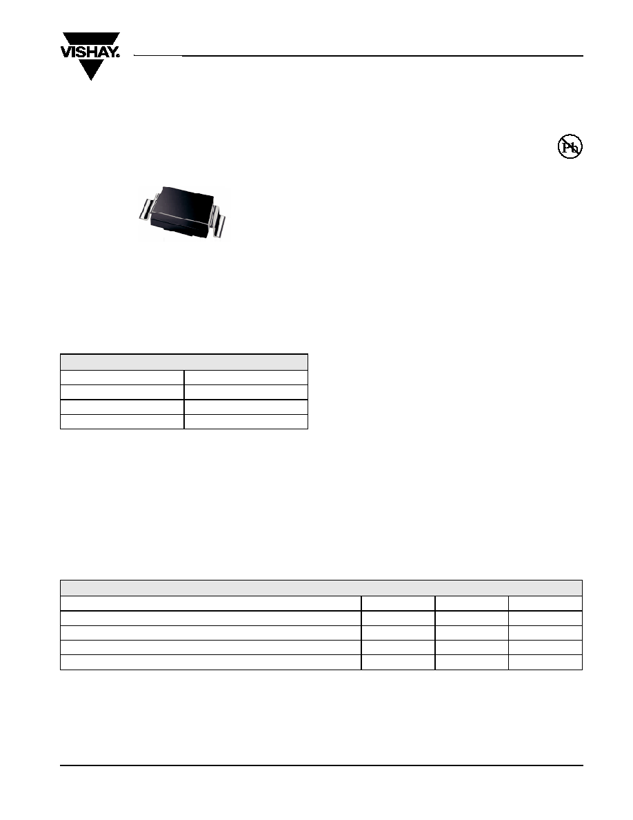
MECHANICAL DATA
Case: DO-215AA (SMBG)
Epoxy meets UL 94V-0 flammability rating
Terminals: Matte tin plated leads, solderable per
J-STD-002B and JESD22-B102D
E3 suffix for commercial grade, HE3 suffix for high
reliability grade (AEC Q101 qualified)
Polarity: For unidirectional types the band denotes
cathode end, no marking on bidirectional types
DO-215AA (SMBG)
DEVICES FOR BIDIRECTION APPLICATIONS
For bidirectional devices use C or CA suffix
(e.g. SMBG10CA).
Electrical characteristics apply in both directions.
MAJOR RATINGS AND CHARACTERISTICS
V
WM
5.0 V to 188 V
P
PPM
600 W
I
FSM
(Unidirectional only)
100 A
T
j
max.
150 ∞C
Note:
(1) Non-repetitive current pulse, per Fig. 3 and derated above T
A
= 25 ∞C per Fig. 2
(2) Mounted on 0.2 x 0.2" (5.0 x 5.0 mm) copper pads to each terminal
MAXIMUM RATINGS (T
A
= 25 ∞C unless otherwise noted)
PARAMETER
SYMBOL
VALUE
UNIT
Peak pulse power dissipation with a 10/1000 µs waveform
(1,2)
(see Fig. 1)
P
PPM
Minimum
600 W
Peak pulse current with a 10/1000 µs waveform
(1)
I
PPM
see next table
A
Peak forward surge current 8.3 ms single half sine-wave uni-directional only
(2)
I
FSM
100 A
Operating junction and storage temperature range
T
J
, T
STG
- 55 to + 150
∞C
www.vishay.com
2
Document Number 88456
05-Jul-06
Vishay General Semiconductor
SMBG5.0 thru SMG188CA
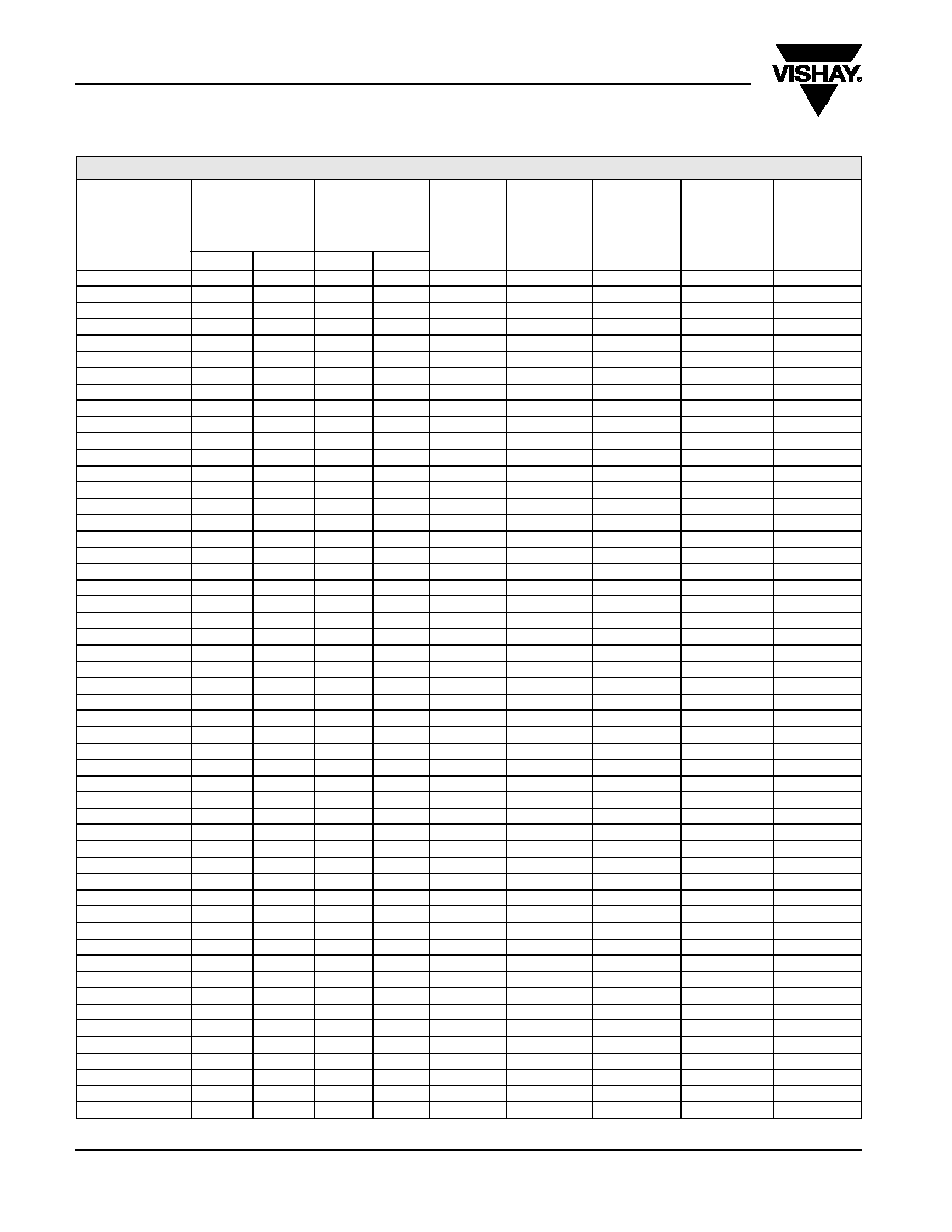
ELECTRICAL CHARACTERISTICS (T
A
= 25 ∞C unless otherwise noted)
DEVICE TYPE
MODIFIED
GULL WING
DEVICE MARKING
CODE
BREAKDOWN
VOLTAGE
V
(BR)
AT I
T
(1)
(V)
TEST
CURRENT
I
T
(mA)
STAND-OFF
VOLTAGE
V
WM
(V)
MAXIMUM
REVERSE
LEAKAGE
AT V
WM
I
D
(µA)
(3)
MAXIMUM
PEAK PULSE
SURGE
CURRENT
I
PPM
(A)
(2)
MAXIMUM
CLAMPING
VOLTAGE AT
I
PPM
V
C
(V)
UNI
BI
MIN MAX
(+)
SMBG5.0
KD KD 6.40
7.82 10
5.0
800
62.5
9.6
(+)
SMBG5.0A
(5)
KE KE 6.40
7.07 10
5.0
800
65.2
9.2
(+)
SMBG6.0
KF KF
6.67
8.15 10
6.0
800
52.6
11.4
(+)
SMBG6.0A
KG KG 6.67
7.37 10
6.0
800
58.3
10.3
(+)
SMBG6.5
KH AH 7.22
8.82 10
6.5
500
48.8
12.3
(+)
SMBG6.5A
KK AK 7.22
7.98 10
6.5
500
53.6
11.2
(+)
SMBG7.0
KL KL
7.78
9.51 10
7.0
200
45.1
13.3
(+)
SMBG7.0A
KM KM 7.78
8.60 10
7.0
200
50.0
12.0
(+)
SMBG7.5
KN AN 8.33
10.2 1.0
7.5
100
42.0
14.3
(+)
SMBG7.5A
KP AP 8.33
9.21 1.0
7.5
100
46.5
12.9
(+)
SMBG8.0
KQ AQ 8.89
10.9 1.0
8.0
50
40.0
15.0
(+)
SMBG8.0A
KR AR 8.89
9.83 1.0
8.0
50
44.1
13.6
(+)
SMBG8.5
KS AS 9.44
11.5 1.0
8.5
20
37.7
15.9
(+)
SMBG8.5A
KT AT
9.44
10.4 1.0
8.5
20
41.7
14.4
(+)
SMBG9.0
KU AU 10.0
12.2 1.0
9.0
10
35.5
16.9
(+)
SMBG9.0A
KV AV 10.0
11.1 1.0
9.0
10
39.0
15.4
(+)
SMBG10
KW AW 11.1
13.6 1.0
10
5.0
31.9
18.8
(+)
SMBG10A
KX AX 11.1
12.3 1.0
10
5.0
35.3
17.0
(+)
SMBG11
KY KY 12.2
14.9 1.0
11
5.0
29.9
20.1
(+)
SMBG11A
KZ KZ
12.2
13.5 1.0
11
5.0
33.0
18.2
(+)
SMBG12
LD BD
13.3
16.3 1.0
12
5.0
27.3
22.0
(+)
SMBG12A
LE BE
13.3
14.7 1.0
12
5.0
30.2
19.9
(+)
SMBG13
LF LF
14.4
17.6 1.0
13
1.0
25.2
23.8
(+)
SMBG13A
LG LG 14.4
15.9 1.0
13
1.0
27.9
21.5
(+)
SMBG14
LH BH
15.6
19.1 1.0
14
1.0
23.3
25.8
(+)
SMBG14A
LK BK
15.6
17.2 1.0
14
1.0
25.9
23.2
(+)
SMBG15
LL BL
16.7
20.4 1.0
15
1.0
22.3
26.9
(+)
SMBG15A
LM BM 16.7
18.5 1.0
15
1.0
24.6
24.4
(+)
SMBG16
LN LN
17.8
21.8 1.0
16
1.0
20.8
28.8
(+)
SMBG16A
LP LM
17.8
19.7 1.0
16
1.0
23.1
26.0
(+)
SMBG17
LQ LQ 18.9
23.1 1.0
17
1.0
19.7
30.5
(+)
SMBG17A
LR LR
18.9
20.9 1.0
17
1.0
21.7
27.6
(+)
SMBG18
LS BS
20.0
24.4 1.0
18
1.0
18.6
32.2
(+)
SMBG18A
LT BT
20.0
22.1 1.0
18
1.0
20.5
29.2
(+)
SMBG20
LU LU
22.2
27.1 1.0
20
1.0
16.8
35.8
(+)
SMBG20A
LV LV
22.2
24.5 1.0
20
1.0
18.5
32.4
(+)
SMBG22
LW BW 24.4
29.8 1.0
22
1.0
15.2
39.4
(+)
SMBG22A
LX BX
24.4
26.9 1.0
22
1.0
16.9
35.5
(+)
SMBG24
LY BY
26.7
32.6 1.0
24
1.0
14.0
43.0
(+)
SMBG24A
LZ BZ
26.7
29.5 1.0
24
1.0
15.4
38.9
(+)
SMBG26
MD CD 28.9
35.3 1.0
26
1.0
12.9
46.6
(+)
SMBG26A
ME CE 28.9
31.9 1.0
26
1.0
14.3
42.1
(+)
SMBG28
MF MF 31.1
38.0 1.0
28
1.0
12.0
50.0
(+)
SMBG28A
MG MG 31.1
34.4 1.0
28
1.0
13.2
45.4
(+)
SMBG30
MH CH 33.3
40.7 1.0
30
1.0
11.2
53.5
(+)
SMBG30A
MK CK 33.3
36.8 1.0
30
1.0
12.4
48.4
(+)
SMBG33
ML CL 36.7
44.9 1.0
33
1.0
10.2
59.0
(+)
SMBG33A
MM CM 36.7
40.6 1.0
33
1.0
11.3
53.3
(+)
SMBG36
MN CN 40.0
48.9 1.0
36
1.0
9.3
64.3
(+)
SMBG36A
MP CP 40.0
44.2 1.0
36
1.0
10.3
58.1
(+)
SMBG40
MQ CQ 44.4
54.3 1.0
40
1.0
8.4
71.4
(+)
SMBG40A
MR CR 44.4
49.1 1.0
40
1.0
9.3
64.5
Document Number 88456
05-Jul-06
www.vishay.com
3
SMBG5.0 thru SMG188CA
Vishay General Semiconductor
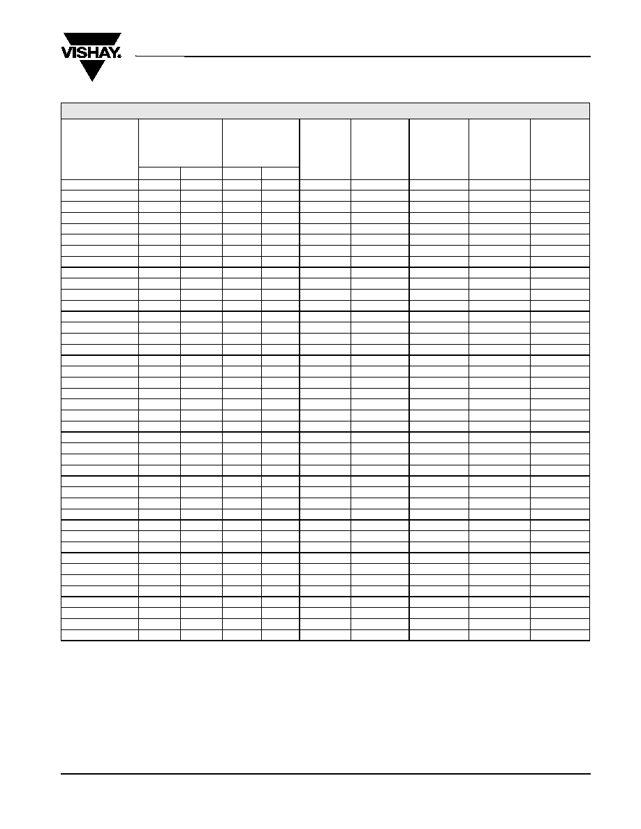
Note:
(1) Pulse test: t
p
50 ms
(2) Surge current waveform per Fig. 3 and derate per Fig. 2
(3) For bi-directional types having V
WM
of 10 Volts and less, the I
D
limit is doubled
(4) All terms and symbols are consistent with ANSI/IEEE C62.35
(5) For the bi-directional SMBG/SMBJ5.0CA, the maximum V
(BR)
is 7.25 V
(6) V
F
= 3.5 V at I
F
= 50 mA (uni-directional only)
(+)
Underwriters Laboratory Recognition for the classification of protectors (QVGQ2) under the UL standard for safety 497B and file number
E136766 for both uni-directional and bi-directional devices
(+)
SMBG43
MS CS 47.8
58.4 1.0
43
1.0
7.8
76.7
(+)
SMBG43A
MT CT 47.8
52.8 1.0
43
1.0
8.6
69.4
(+)
SMBG45
MU MU 50.0
61.1 1.0
45
1.0
7.5
80.3
(+)
SMBG45A
MV MV 50.0
55.3 1.0
45
1.0
8.3
72.7
(+)
SMBG48
MW MW 53.3
65.1 1.0
48
1.0
7.0
85.5
(+)
SMBG48A
MX MX 53.3
58.9 1.0
48
1.0
7.8
77.4
(+)
SMBG51
MY MY 56.7
69.3 1.0
51
1.0
6.6
91.1
(+)
SMBG51A
MZ MZ 56.7
62.7 1.0
51
1.0
7.3
82.4
(+)
SMBG54
ND ND 60.0
73.3 1.0
54
1.0
6.2
96.3
(+)
SMBG54A
NE NE 60.0
66.3 1.0
54
1.0
6.9
87.1
(+)
SMBG58
NF NF 64.4
78.7 1.0
58
1.0
5.8
103
(+)
SMBG58A
NG NG 64.4
71.2 1.0
58
1.0
6.4
93.6
(+)
SMBG60
NH NH 66.7
81.5 1.0
60
1.0
5.6
107
(+)
SMBG60A
NK NK 66.7
73.7 1.0
60
1.0
6.2
96.8
(+)
SMBG64
NL NL
71.1
86.9 1.0
64
1.0
5.3
114
(+)
SMBG64A
NM NM 71.1
78.6 1.0
64
1.0
5.8
103
(+)
SMBG70
NN NN 77.8
95.1 1.0
70
1.0
4.8
125
(+)
SMBG70A
NP NP 77.8
86.0 1.0
70
1.0
5.3
113
(+)
SMBG75
NQ NQ 83.3
102 1.0
75
1.0
4.5
134
(+)
SMBG75A
NR NR 83.3
92.1 1.0
75
1.0
5.0
121
(+)
SMBG78
NS NS 86.7
106 1.0
78
1.0
4.3
139
(+)
SMBG78A
NT NT 86.7
95.8 1.0
78
1.0
4.8
126
(+)
SMBG85
NU NU 94.4
115 1.0
85
1.0
4.0
151
(+)
SMBG85A
NV NV 94.4
104 1.0
85
1.0
4.4
137
(+)
SMBG90
NW NW 100 122 1.0
90
1.0
3.8
160
(+)
SMBG90A
NX NX 100
111 1.0
90
1.0
4.1
146
(+)
SMBG100
NY NY 111
136 1.0
100
1.0
3.4
179
(+)
SMBG100A
NZ NZ 111
123 1.0
100
1.0
3.7
162
(+)
SMBG110
PD PD 122
149 1.0
110
1.0
3.1
196
(+)
SMBG110A
PE PE 122
135 1.0
110
1.0
3.4
177
(+)
SMBG120
PF PF 133
163 1.0
120
1.0
2.8
214
(+)
SMBG120A
PG PG 133
147 1.0
120
1.0
3.1
193
(+)
SMBG130
PH PH 144
176 1.0
130
1.0
2.6
231
(+)
SMBG130A
PK PK 144
159 1.0
130
1.0
2.9
209
(+)
SMBG150
PL PL 167
204 1.0
150
1.0
2.2
268
(+)
SMBG150A
PM PM 167
185 1.0
150
1.0
2.5
243
(+)
SMBG160
PN PN 178
218 1.0
160
1.0
2.1
287
(+)
SMBG160A
PP PP 178
197 1.0
160
1.0
2.3
259
(+)
SMBG170
PQ PQ 189
231 1.0
170
1.0
2.0
304
(+)
SMBG170A
PR PR 189
209 1.0
170
1.0
2.2
275
SMBG188 PT
PT
209
255
1.0
188 1.0 1.7 344
SMBG188A PS
PS
209
231
1.0 188 1.0
2.0 328
ELECTRICAL CHARACTERISTICS (T
A
= 25 ∞C unless otherwise noted)
DEVICE TYPE
MODIFIED
GULL WING
DEVICE MARKING
CODE
BREAKDOWN
VOLTAGE
V
(BR)
AT I
T
(1)
(V)
TEST
CURRENT
I
T
(mA)
STAND-OFF
VOLTAGE
V
WM
(V)
MAXIMUM
REVERSE
LEAKAGE
AT V
WM
I
D
(µA)
(3)
MAXIMUM
PEAK PULSE
SURGE
CURRENT
I
PPM
(A)
(2)
MAXIMUM
CLAMPING
VOLTAGE AT
I
PPM
V
C
(V)
UNI
BI
MIN MAX
www.vishay.com
4
Document Number 88456
05-Jul-06
Vishay General Semiconductor
SMBG5.0 thru SMG188CA
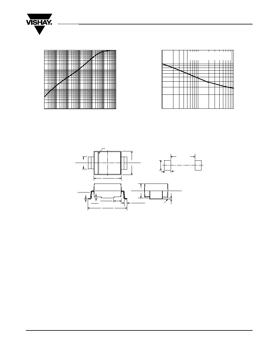
RATINGS AND CHARACTERISTICS CURVES
(T
A
= 25
∞C unless otherwise noted)
THERMAL CHARACTERISTICS (T
A
= 25 ∞C unless otherwise noted)
PARAMETER
SYMBOL
VALUE
UNIT
Typical thermal resistance, junction to ambient
R
JA
100 ∞C/W
Typical thermal resistance, junction to lead
R
JL
20 ∞C/W
ORDERING INFORMATION
PREFERRED P/N
UNIT WEIGHT (g)
PREFERRED PACKAGE CODE
BASE QUANTITY
DELIVERY MODE
SMBG5.0A-E3/52
0.096
52
750
7" Diameter Plastic Tape & Reel
SMBG5.0A-E3/5B
0.096
5B
3200
13" Diameter Plastic Tape & Reel
Figure 1. Peak Pulse Power Rating Curve
Figure 2. Pulse Power or Current versus Initial Junction Temperature
0.1
1
10
100
0.2 x 0.2" (0.5 x 0.5 mm)
Copper Pad Areas
P
PPM
- P
e
ak P
u
lse P
o
w
er (k
W
)
td - Pulse Width (s)
0.1 µs
1.0 µs
10 µs
100 µs
1.0 ms
10 ms
0
25
50
75
100
100
75
50
25
0
125
150
175
200
T
J
- Initial Temperature (∞C)
P
eak P
u
lse P
o
w
er (P
PP
) or C
u
rrent (I
PP
)
Der
ating in P
ercentage
,
%
Figure 3. Pulse Waveform
Figure 4. Typical Junction Capacitance
0
50
100
150
td
0
1.0
2.0
3.0
4.0
tr = 10 µsec
Peak Value
I
PPM
Half Value -
I
PPM
IPP
2
10/1000 µsec Waveform
as defined by R.E.A.
T
j
= 25 ∞C
Pulse Width (td)
is defined as the point
where the peak current
decays to 50 % of I
PPM
I
PPM
- P
eak P
u
lse C
u
rrent,
%
I
RSM
t - Time (ms)
10
100
1000
6000
10
1
100
200
Uni-Directional
Bi-Directional
T
j
= 25 ∞C
f = 1.0 MHz
V
sig
= 50 mVp-p
Measured at
Zero Bias
V
R
, Measured at
Stand-off
Voltage V
WM
C
J
- J
u
nction Capacitance (pF)
V
WM
- Reverse Stand-off Voltage (V)
Vishay General Semiconductor
SMBG5.0 thru SMG188CA
Document Number 88456
05-Jul-06
www.vishay.com
5
PACKAGE OUTLINE DIMENSIONS in inches (millimeters)
Figure 5. Typical Transient Thermal Impedance
0.1
1.0
10
100
0.001
0.01
0.1
10
1
100
1000
tp - Pulse Duration (s)
T
r
ansient Ther
mal Impedance (∞C/
W
)
Figure 6. Maximum Non-Repetitive Peak Forward Surge Current
10
200
100
1
100
10
Number of Cycles at 60 Hz
P
eak F
o
r
w
ard S
u
rge C
u
rrent (A)
8.3 ms Single Half Sine-Wave
Unidirectional Only
0.180 (4.57)
0.160 (4.06)
0.016 (0.41)
0.006 (0.15)
0.020
(0.51) Max.
0.058 (1.47)
0.038 (0.97)
0.255 (6.48)
0.235 (5.97)
0.030 (0.76)
0.015 (0.38)
0.008 (0.20)
0.004 (0.10)
SEATING
PLANE
0.155 (3.94)
0.130 (3.30)
0.083 (2.10)
0 .077 (1.96)
0.095 (2.41)
0.075 (1.90)
0.165 (4.19)
0.085 (2.16)
0.060 (1.27)
DO-215AA (SMBG)
Mounting Pad Layout
Cathode Band