V C X O
VF596E
75 South Street, Hopkinton, MA 01748 800-982-5737 508-435-6831 Fax: 508-435-5289 www.valpeyfisher.com
88
VF596E
ECLinPS
TM
Compatible Surface Mount
VCXO for 3.3 Volt Applications
F E AT U R E S
∑
Wide and High Frequency Range
∑
Wide Pull Range Available
∑
No Frequency Multiplication is
Used: Very Low Phase Jitter
∑
Complementary Output Standard
∑
Fundamental Crystal Design
Parameter
Symb
Condition
Min
Typ
Max
Unit
Note
Input Break
Vcc
≠0.5
7.0
V
Down Voltage
Storage Temp.
Ts
≠55
+85
∞C
Control Voltage
Vc
≠1
9
V
Frequency
Range
F
12.5
200
MHz
Frequency
F/F
Vs. Vcc, Temp.
±25
ppm
Stability
Input Voltage
Vcc
4.75
5.00
5.25
V
Std.
3.15
3.30
3.45
LV Opt.
Input Current
Icc/Iee
50 Ohm Load
65
mA
Duty Cycle
@50%
45
50
55
%
Load
@50%
45
50
55%
Rise/Fall Time
Tr/Tf
20% to 80%
0.6
ns
Logic "1" Level
Voh
Vcc≠
Vcc≠
V
0.96
0.81
Logic "0" Level
Vol
Vcc≠
Vcc≠
V
1.85
1.65
Start≠up Time
Ts
2
10
ms
Phase Jitter
1
1
ps
fj>1KHz
Modulation BW
fm
@Vc = 2.5V
10
KHz
@≠3db
Input Impedance
fm<10KHz
50
KOhm
Control Voltage
Vc
0
3.3
V
Deviation
Vc = 0V to 3.3V,
±100
ppm
25∞C
Absolute Usable
APR
Overall
±50
ppm
Pull Range
Deviation Slope
Monotonic,
50
ppm/V
positive
Linearity ±20
%
1
Setability (Vc
Vc0
@25∞C, Fnom.
1.25
1.65
2.05
V
for center freq)
Enable/
Disable Function
Enable/ Te/Td
100
ns
Disable Time
Operating
Temperature Range
0∞C to +70∞C (≠40∞C to +85∞C available)
Mechanical Shock
Per MIL≠STD≠202, Method 213, Cond. E
Thermal Shock
Per MIL≠STD≠883, Method 1011, Cond. A
Vibration
Per MIL≠STD≠883, Method 2007, Cond. A
Soldering Conditions
260∞C, for 10s, Max., or 230∞C for 90s Max.
Hermetic Seal
Leak rate less than 5 x 10
≠8
atm.cc/s of helium
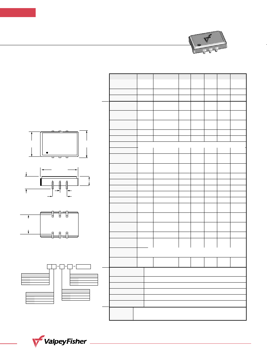
Pin Out
Pin #1≠Voltage Control
Pin #2≠Negative Enable (internal pulldown)
Pin #3≠Ground, Case
Pin #4≠Output
Pin #5≠Complementary Output Pin #6≠Vcc
50 Ohm to Vcc≠2V or Thevenin Equiv. Bias Required
Absolute
Max. Ratings
Electrical
Environmental and Mechanical
Electrical
Connections
Input HIGH (>2.5V)
DISABLED
Input LOW (<0.5V): or floating:
ACTIVE
0.550" TYP.
(13,97mm)
0.385"
(9,78mm)
0.200"
(5,08mm)
0.100"
(2,54mm)
0.130" TYP.
(3,302 mm)
0.185"
MAX.
(4,70mm)
0.350"
(8,89mm)
VF596E
155.520MHZ
I
O1H
0.300"
(7,62 mm)
Mounting Center
1
2
3
6
5
4
1
Creating a Part Number
VF596E
ABSOLUTE PULL RANGE
Code
Specification
±
100 ppm MIN. (std.)
XXX
specify deviation MIN.
(up to
±
200 ppm MAX.)
FREQUENCY STABILITY
Code
Specification
S
±
20 ppm
±
25 ppm
OPERATIONAL TEMP. RANGE
Code
Specification
0
∞
C to +70
∞
C (std.)
1 -40
∞
C to +85
∞
C
Example: VF596ES-1-50-155.520MHz: Frequency Stability
±
20ppm, Duty
Cycle
±
5.0%, Input Voltage 3.3 Volt
±
5%, Operational Temperature -45
∞
C to
+85
∞
C, Complementary Output, APR
±
50ppm, Frequency 155.520MHz.
FREQ.
INPUT VOLTAGE
Code
Specification
L 3.3
Volt
±
5%
5.0
Volt
±
5% (std.)
Note: Tighter linearity specification available.
All specifications are subject to change without notice.
All dimensions are typical unless otherwise specified.