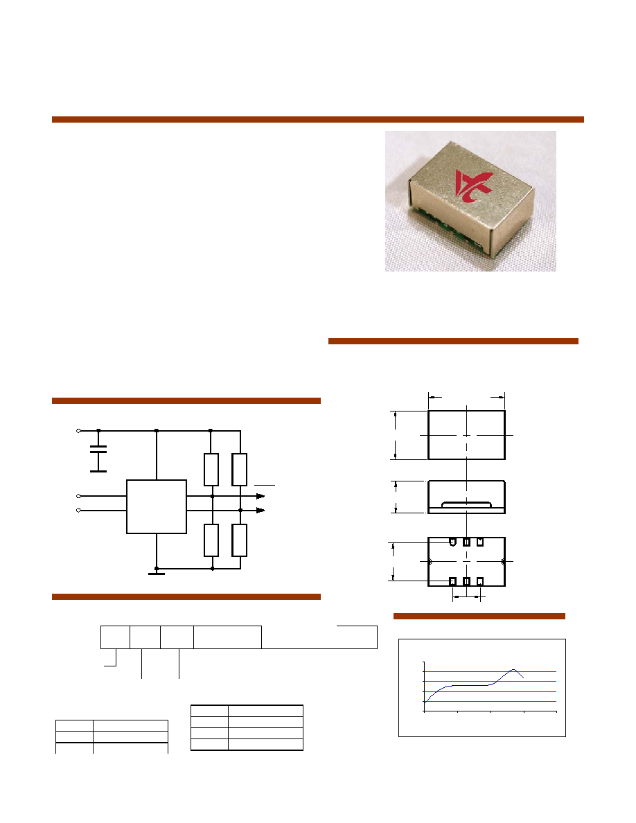
VFT5 Series Surface Mount UHF VCXO
COOL...TO THE TOUCH
Product Data Sheet
Features
∑ Small, Low Profile SMD Package
∑ Very Low Phase Jitter and Phase Noise
∑ Excellent Frequency Stability
∑ Low Aging, Vacuum sealed Crystal
∑ Complementary Output Standard
∑ Enable/Disable Standard
∑ Very High Frequency
∑ Available as a CLOCK, add "C" to part #
Applications
∑ Optical Networking, SONET/SDH
∑ 10 Gbit Ethernet
∑ Frequency Translation
SMD Reflow Profile
0
50
100
150
200
250
0
50
100
150
200
Time, s
Temperature, ∞C
0.55 (14 mm)
0.35 (9 mm)
0.24 (6.1 mm)
0.200 (5.08 mm)
0.300 (7.62 mm)
1 2
3
4
5
6
Creating a Part Number
VFT5
FREQUENCY, MHz
Temperature Range
Code Specification
A
-10∞C to 60∞C
B
0∞C to 70∞C
C
-40∞C to 85∞C
Supply Voltage
Code Specification
S 5V
±5%
L 3.3V
±5%
C for
clock
-APR, ppm
5
4
2
3
1
OUTPUT
Vcc
GND
DUT
OUTPUT
6
Vc
En/Dis
5V
82 Ohm
82 Ohm
120 Ohm
120 Ohm
VF Technologies
∑ 75 South Street, Hopkinton, MA 01748 ∑ Tel. 1-800-XTALREP, 508-435-6831 ∑ FAX 508 4355289
1

VFT5 Series Surface Mount UHF VCXO
Specifications
Parameter
Symb Condition
Min Typ Max Unit
Note
Absolute Maximum Ratings
Input Break
Down Voltage
Vcc
-0.5
7.0
V
Storage temp.
Ts -55
85
∞
C
Contr. Voltage
Vc
-1
9
V
Electrical
Frequency
range
F 600
960
MHz
Input Voltage
Vcc 4.75
3.15
5.00
3.30
5.25
3.45
V Std
LV
Input Current
Icc
50 Ohm Load
75
mA
Frequency
Stability
F/F
vs. Temperature
vs. Vcc
aging
±20
±5
±5
ppm
ppm/V
ppm/year
First Year
Load
50 Ohm to Vcc-2V or Thevenin Equiv. Bias Required
Duty cycle
@50% 45
50
55
%
Rise/Fall time
Tr/Tf
20 to 80 %
0.6
ns
Logic "1" level
Voh
Vcc-0.96 Vcc-0.81 V
Logic "0" level
Vol
Vcc-1.85 Vcc-1.65 V
Start up time
Ts
2
10
ms
Phase jitter
1
1
ps fj>1KHz,
also valid for 50
KHz to 80 Mhz
SSB Phase Noise
@100
Hz
@1 KHz
@10 KHz
@100 KHz
-85
-115
-125
-135
dBc/Hz
Modulation BW fm @Vc=2.5V
>10KHz
@-3db
Input
Impedance
fm < 10KHz
> 50Kohm
Control voltage
Vc
0
0
5
3.3
V Std
LV
Deviation
Vc=0V to 5V,25∞C
Vc=0V to 3.3V,25∞C
±100 ppm
Absolute usable
pull range
Over
all ±50 ppm
1
Deviation slope
Monotonic,
positive
50
ppm/V
Linearity
-10
+10
%
Setability (Vc
for center freq.)
Vc0 @25∞C,
Fnom.
2.0
1.25
2.5
1.65
3.0
2.05
V Std
LV
Enable/disable
Function
Input HIGH (>2.5V): DISABLED
Input LOW (<0.5V) or floating: ACTIVE
Enable/disable
Time
Te/Td
100
ns
Environmental and Mechanical
Operating temp.
range
0∞C to 70∞C (-40∞C to 85∞C available)
Mechanical Shock
Per MIL-STD-202, Method 213, Cond. E
Thermal Shock
Per MIL-STD-883, Method 1011, Cond. A
Vibration
Per MIL-STD-883, Method 2007, Cond. A
Soldering Conditions
230∞C for 90s Max
Hermetic Seal
Leak rate less than 5x10⁻⁸ atm.cc/s of helium (crystal only)
Electrical Connections
Pin Out
Pin #1- Voltage Control Pin #2 - Negative Enable (internal pulldown)
Pin #3 - Case, Gnd Pin #4 - Output
Pin #5 - Complementary Output Pin #6 - Vcc
VF Technologies
∑ 75 South Street, Hopkinton, MA 01748 ∑ Tel. 1-800-XTALREP, 508-435-6831 ∑ FAX 508 4355289
2
Notes: 1. Up to 100 ppm available at Vcc = 5V