Äîêóìåíòàöèÿ è îïèñàíèÿ www.docs.chipfind.ru
88
Vectron International · 267 Lowell Road, Hudson, NH 03051 · Tel: 1-88-VECTRON-1 · Web: www.vectron.com
FX-200
Description:
The FX-200 is a dual output frequency translator which is used to translate
one of two different input frequencies greater than 1 MHz to one of two dif-
ferent output frequencies between 77.76 MHz and 777.6 MHz. All the major
FEC rates are supported such as 15/14ths and 255/237. This unit can also
support switching from 10.0 G to 10.3125 G, or even OC-n to 10 GigE.
Applications:
· SONET/SDH
· DWDM
· FEC (Forward Error Correction)
Output Frequencies
77.76
777.6
MHz
Supply Voltage,
C = 5.0 Vdc
V
cc
4.75
5.00
5.25
Vdc
D = 3.3 Vdc
V
cc
3.15
3.30
3.45
Vdc
Supply Current
5.0 Vdc
Icc
80
125
mA
3.3 Vdc
Icc
75
120
mA
Input Signal,
Comp PECL
CLKIN
PECL
---
OUTPUT,
F = Comp PECL
---
---
PECL
---
---
V
OH
(Temp Range C = 0°C to +70°C)
V
OH
V
cc
-1.025
V
cc
-0.880
V
V
OL
(Temp Range C = 0°C to +70°C)
V
OL
V
cc
-1.810
V
cc
-1.620
V
V
OH
(Temp Range F = -40°C to +85°C)
V
OH
V
cc
-1.085
V
cc
-0.880
V
V
OL
(Temp Range F = -40°C to +85°C)
V
OL
V
cc
-1.830
V
cc
-1.555
V
Rise/Fall Time
(20% to 80% @ 622.08 MHz)
t
R
/t
F
250
400
ps
Output Symmetry (Duty Cycle)
Sym
45
49/51
55
%
Jitter Generation, rms
(12kHz to 20 MHz)
0.23
1
ps
Jitter Generation, rms
(cycle to cycle method)
3
5
ps
Jitter Transfer, GR-253-CORE sec 5.6.2.1.2
0.1
dB
Input Frequency Tracking Capability
(Can translate Stratum 1,2,3,3E,4 or SONET Min. source)
APR
±40
ppm
Operating Temperature
Temp Range C = 0°C to +70°C
Temp Range F = -40°C to +85°C
Package Size
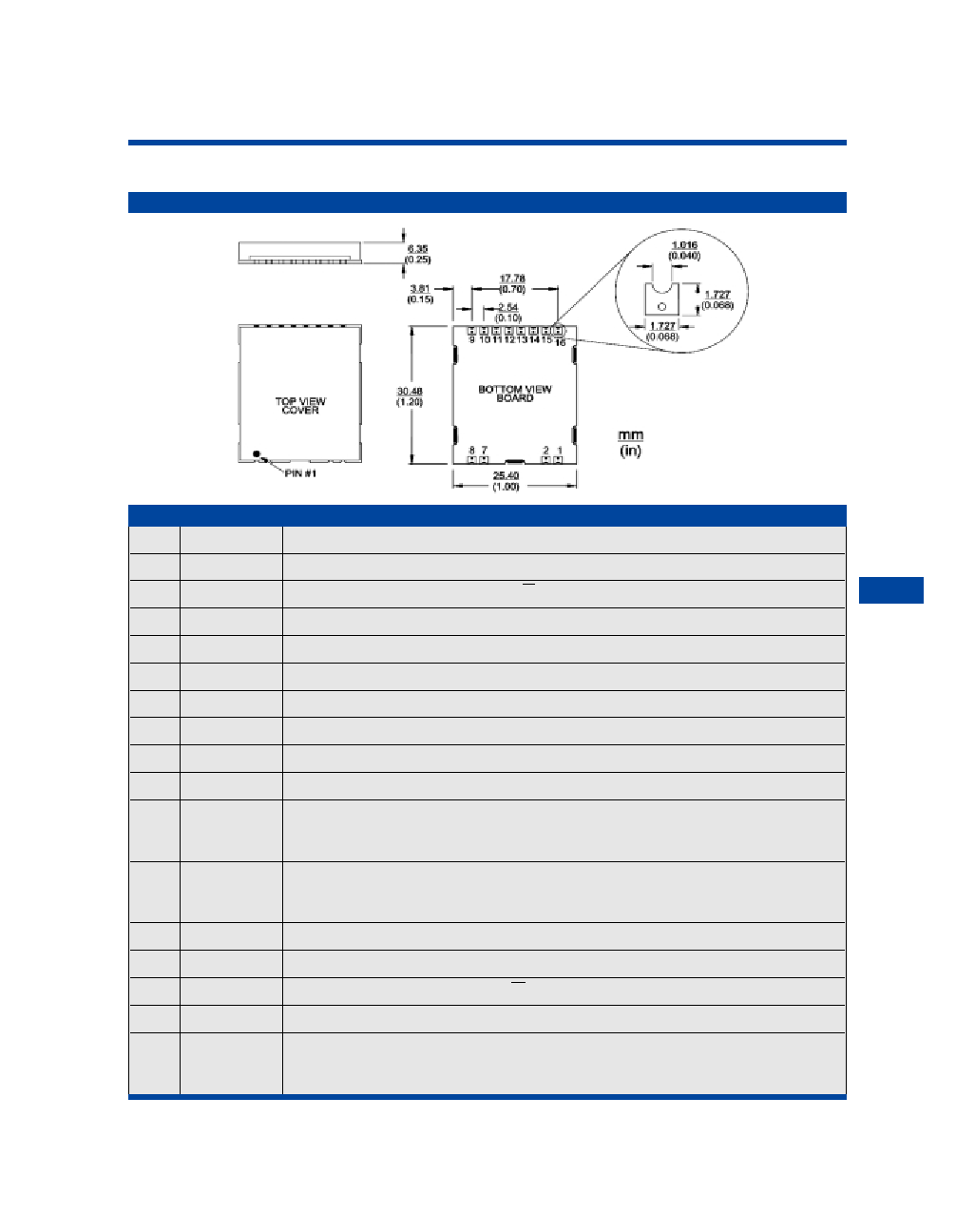
30.48 x 25.4 x 6.35 mm (1.2" x 1.0 x 0.25")
Performance Characteristics
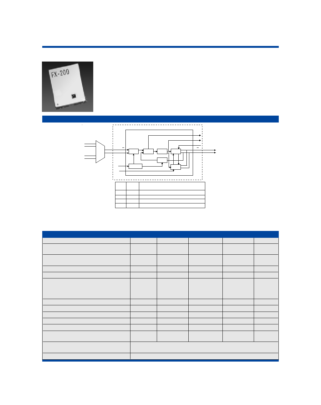
Typical Application
All components outside the dotted line box are user supplied components. This is just one possible
configuration of the FX-200. For additional information about your specific needs, please contact our factory.
Loop Filter
Disable
Lock Detect
FX-200
Phase Freq
Detector
PECL
VCSO 1
VCXO Monitor
Frequency
Divider
Microprocessor
Frequency
Divider
Input
Frequency
Output
Select
Q
Q
Q
Q
PECL
VCSO 2
Input
Select
A) 155.52 MHz
B) 166.6286 MHz
1) 622.08 MHz
2) 666.5143 MHz
Input Signal
Output Signal
Input
Select!
0
0
1
1
Output
Select!
0
1
0
1
Description of Action!
A to 1 :Translates 155.5200 MHz to 622.0800 MHz
A to 2 :Translates 155.5200 MHz to 666.5143 MHz!
B to 1 :Translates 166.6286 MHz to 622.08 MHz!
B to 2 :Translates 166.6286 MHz to 666.5143 MHz!
Parameter Symbol
Min.
Typical
Max
Unit
Frequency Translation Products
PRELIMINAR
Y - AV
AILABLE Q3
8798_AA's Vectron 05/30/02 3:12 PM Page 88
Vectron International · 267 Lowell Road, Hudson, NH 03051 · Tel: 1-88-VECTRON-1 · Web: www.vectron.com
89
FX-200
Pin
Symbol
Function
1
In
Input Frequency
2
CIn
Complementary Input Frequency (Q)
3
---
Missing
4
---
Missing
5
---
Missing
6
---
Missing
7
In Sel
Input Select - "0" = A, "1" = B
8
Out Sel
Output Select - "0" = 1, "1" = 2
9
Vcc
Supply Voltage
10
LD
Lock Detect
(output)
Logic "1" indicates a locked condition
Logic "0" indicates that no input signal is presented
11
Monitor
PLL / VCSO control Voltage. Under locked conditions, should be >0.3V and <3.0V
(output)
for the 3.3 volt option or >0.5V and <4.5V for the 5 volt option.
Input frequency may be out of range if voltage exceeds these limits.
12
Out
Output Signal - Q
13
GND
Ground
14
COut
Complementary Output Signal - Q
15
GND
Ground
16
Disable
Disables Output
(input)
Floating and logic "0" = Output Enabled
Logic "1" = Output Disabled
Pin Out Information
Outline Drawing
Frequency Translation Products
F X
8798_AA's Vectron 05/30/02 3:12 PM Page 89
90
Vectron International · 267 Lowell Road, Hudson, NH 03051 · Tel: 1-88-VECTRON-1 · Web: www.vectron.com
FX-200
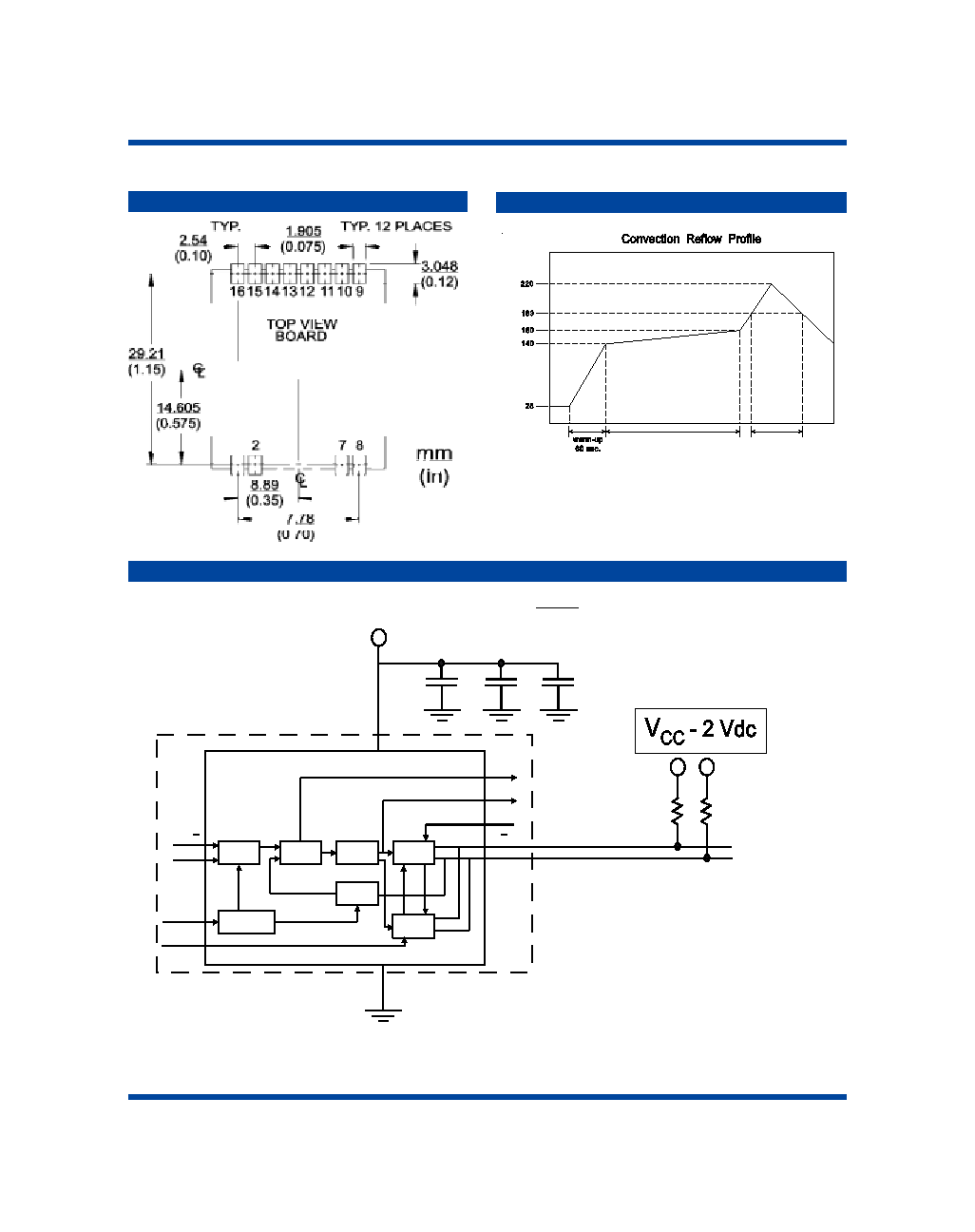
Output Load Configuration
Recommended Pad Layout
Recommended Reflow Profile
pre-heating!
60 to 90 sec.!
@ 140ºC to 160ºC
reflow!
40 to 60 sec.!
@ >183ºC
T
e
mper
atur
e (
º
C
)
V
CC
*
(Fout)
(13,15)
(14)
(9)
*
*
(12)
50 ohms
50 ohms
Loop Filter
Disable
Lock Detect
FX-200
Phase Freq
Detector
PECL
VCSO 1
VCXO Monitor
Frequency
Divider
Microprocessor
Frequency
Divider
Input
Frequency
Output
Select
Q
Q
Q
Q
PECL
VCSO 2
Input
Select
All components outside the dotted line
box are user supplied components
and/or connections. This is just one
possible configuration of the FX-200.
For additional information about your
specific needs please contact our
Factory.
*Note: VI highly recommends either a linear
regulator or bypass capacitors; 10 uF, 0.1 uF
and a 100pF capacitor would be typical.
Frequency Translation Products
8798_AA's Vectron 05/30/02 3:12 PM Page 90
Frequency Translation Products
Vectron International · 267 Lowell Road, Hudson, NH 03051 · Tel: 1-88-VECTRON-1 · Web: www.vectron.com
91
FX-200
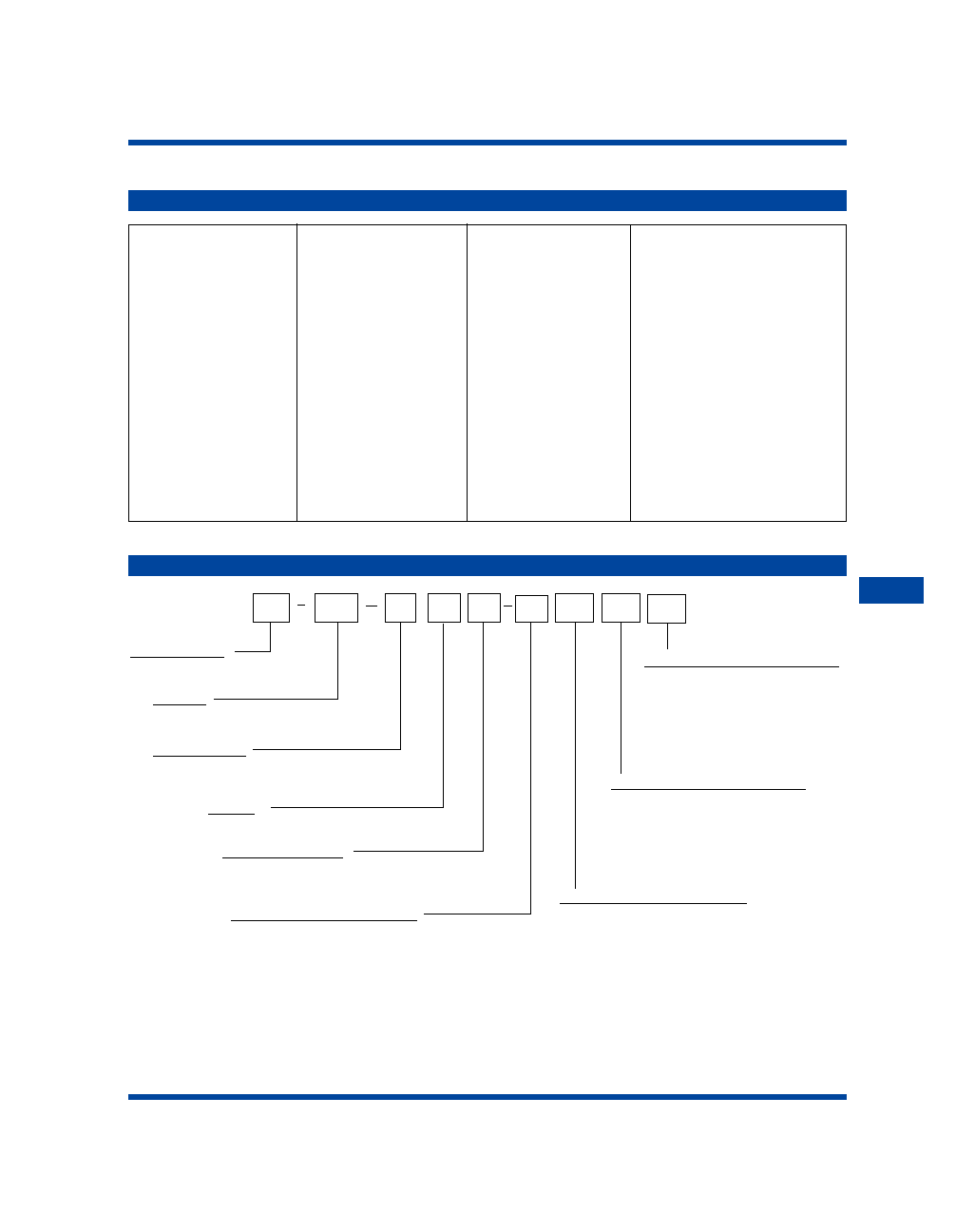
Ordering Information
FX
200
F
D
C
M5
Supply Voltage
C = 5.0 Vdc ±5%
D = 3.3 Vdc ±5%
P2
M2
Output
F = Comp. PECL
Temperature Range
C = 0
o
C to +70
o
C
F = -40
o
C to +85
o
C
Input Frequency - A (B2 to R4)
See Frequency Chart Above
*If not listed enter SS in this block and then
list the frequency after the part number.
**Input A must be less than Input B
Output Frequency - 1 (K2 to T3)
See Frequency Chart Above
*Consult factory for availability of
non-standard output frequencies.
**Output Frequency 1 must be less
than Output Frequency 2.
Input Frequency - B (B3 to R4)
See Frequency Chart Above, for Only 1 input
Frequency Place XX in this location.
*If not listed enter SS in this block and then
list the frequency after the part number.
**Input B must be greater than Input A
Standard Frequencies
1.024 MHz
B2
1.544 MHz
B3
2.048 MHz
B4
4.096 MHz
B5
6.480 MHz
C2
8.192 MHz
C3
10.000 MHz
C4
12.800 MHz
D2
13.000 MHz
D3
15.000 MHz
D4
16.384 MHz
D5
19.440 MHz
D6
20.0000 MHz
E2
20.1416 MHz
E3
20.4800 MHz
E4
22.2171 MHz
E5
26.0000 MHz
F3
27.0000 MHz
F4
29.4912 MHz
F5
32.7680 MHz
H3
37.0560 MHz
H4
38.8800 MHz
H5
44.4343 MHz
J2
44.7360 MHz
J3
51.8400 MHz
J4
61.4400 MHz
J5
65.5360 MHz
J6
77.7600 MHz
K2
78.1250 MHz
K3
78.6432 MHz
K5
82.9440 MHz
K6
112.000 MHz
L2
114.000 MHz
L3
125.000 MHz
L4
139.264 MHz
L5
155.520 MHz
M2
156.250 MHz
M3
161.1328 MHz M4
166.6286 MHz M5
167.3316 MHz N2
168.0407 MHz N3
622.0800 MHz P2
624.7048 MHz
P6
625.0000 MHz
P3
627.3296 MHz
P7
644.5312 MHz
P4
666.5143 MHz
P5
669.1281 MHz
R2
669.3266 MHz
R3
690.5692 MHz
R4
710.9486 MHz
T2
719.7344 MHz T3
777.6000 MHz T4
No Second Input Freq XX
Input Freq not listed
SS
Output Freq not listed SS
P5
Output Frequency - 2 (K3 to T4)
See Frequency Chart Above
*Consult factory for availability of
non-standard output frequencies.
** Output Frequency 2 must be
greater than Output Frequency 1.
*A special part number will be assigned for these cases.
**Input A must be less than Input B. Output 1 must be less than Output 2.
Not all frequency combinations are possible. Please consult factory.
Package
200 = 16 lead SMD
Product Family
FX-Frequency Translator Package
F X
8798_AA's Vectron 05/30/02 3:12 PM Page 91